Archive for the ‘Uncategorized’ Category.

Random SEM Images – MCM68364 64KB ROM

I wanted to make sure the SEM was still happily chugging away so picked up some cheap wafer fragments on eBay and did some imaging. Truth be told, I think I just enjoy throwing things in the SEM and seeing what they look like. If you have something you’d like imaged drop me a line (particularly if you’re from the hacker or maker community) and we can arrange to have it imaged. Currently samples need to be conductive as we don’t have a sputtering machine up and running here yet.

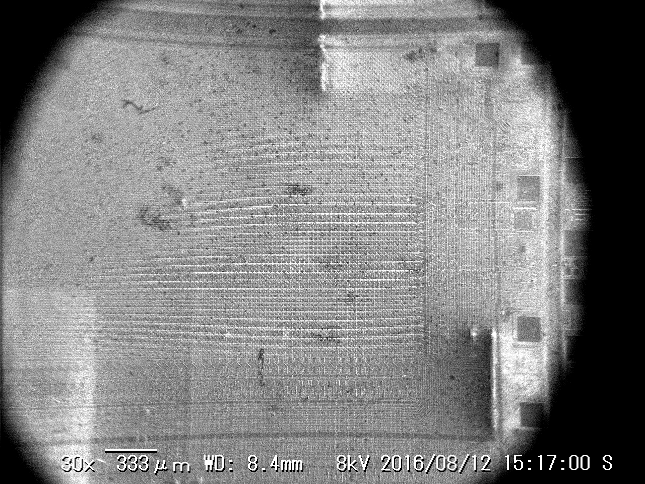
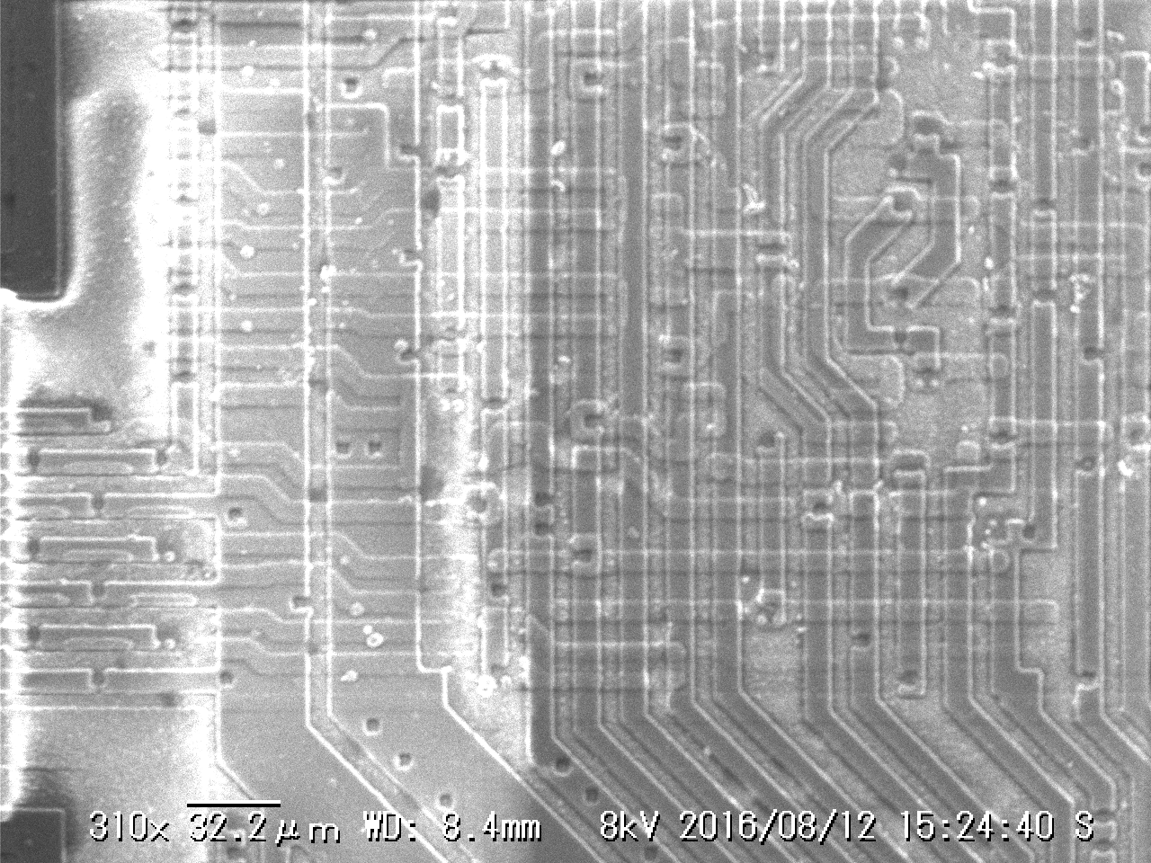
Anyway… on to the images! Here’s a shot at the lowest magnification:

20160812_151700.bmpHonestly, it would probably just be better to use an optical microscope here. And in fact, the features on this chip are relatively big. But I do love the fact that with a SEM you can go all the way from 30x to 20000x.

Here’s a random shot of part of the matrix, I’d guess this is something like a 1 micron process? Maybe sub-micron but not double digit nanometer. Pretty old stuff:

20160812_143924.bmp

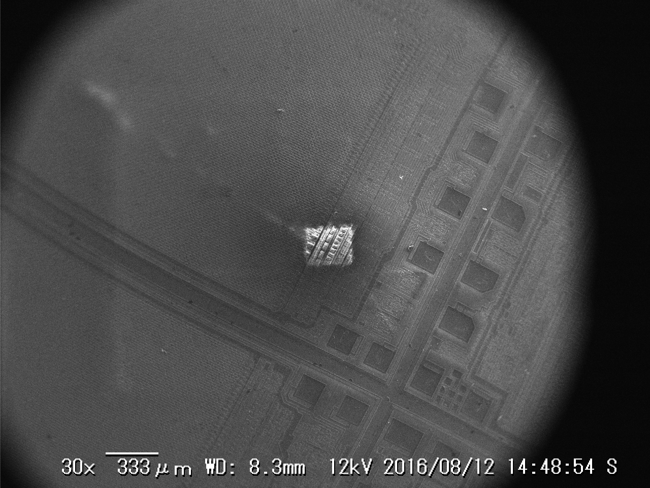
After taking that image I zoomed out a bit. Thing about SEMs is that they’re often somewhat destructive. You can see that the die has been scared in that area. After that shot I lowered the acceleration voltage a bit…

20160812_144854.bmp

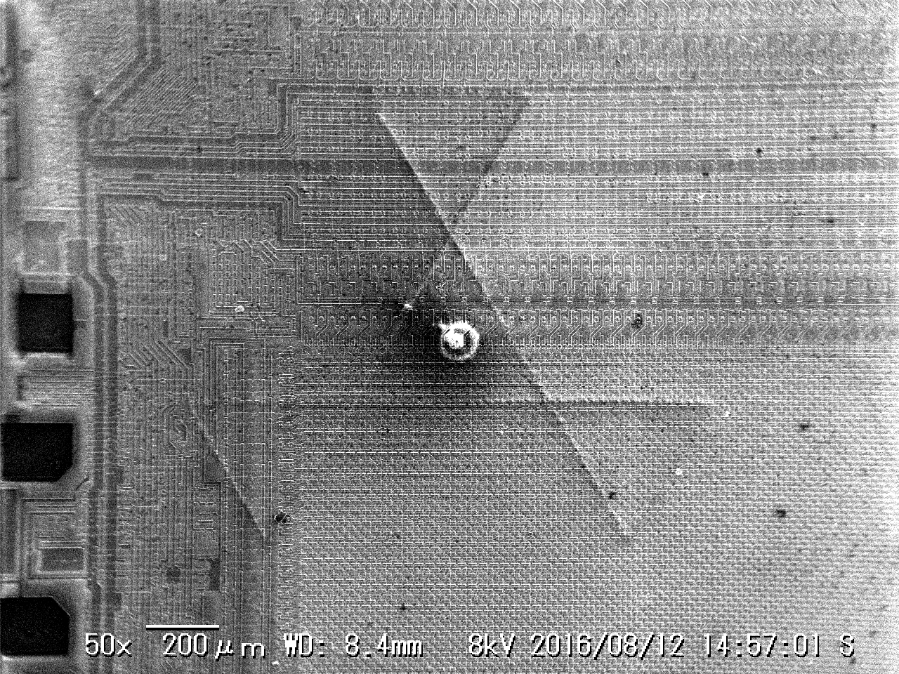
I’m guessing there’s a reason these wafers found their way onto eBay and not into a product.I assume this marking was produced by test jig to mark dies as faulty:

20160812_145701.bmp

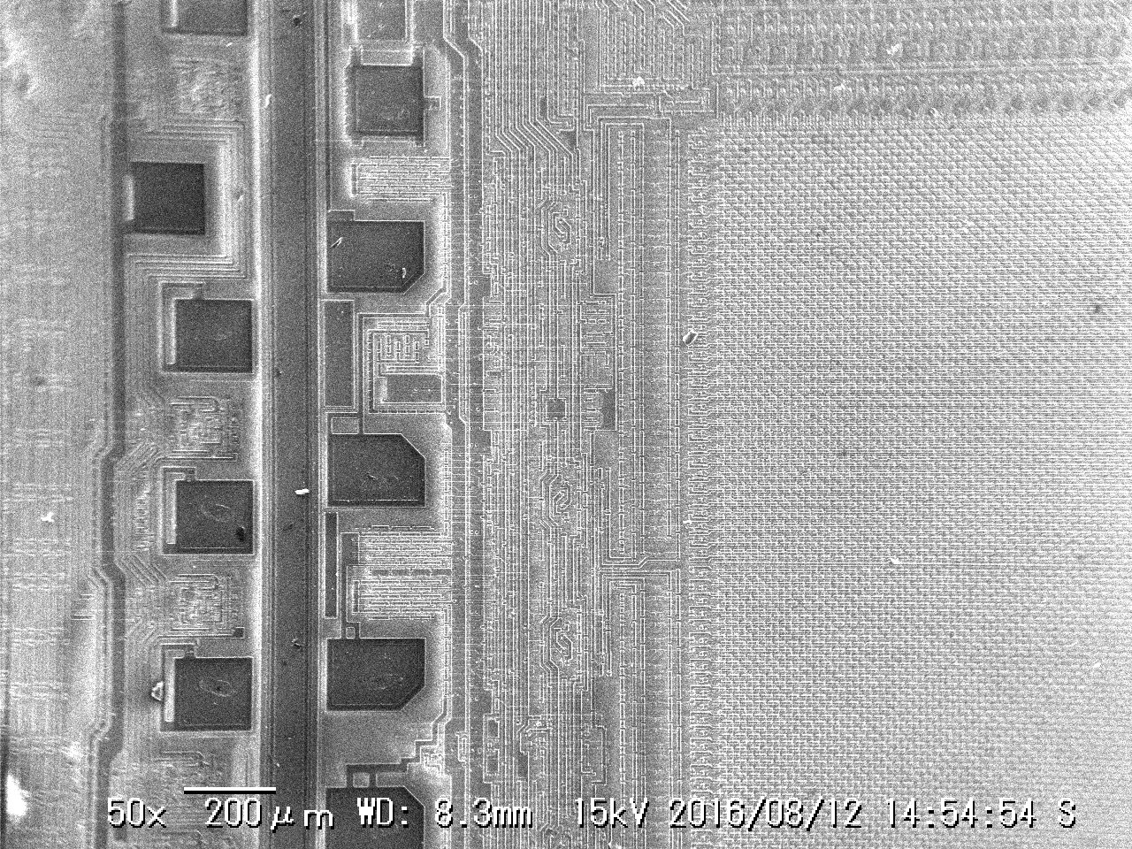
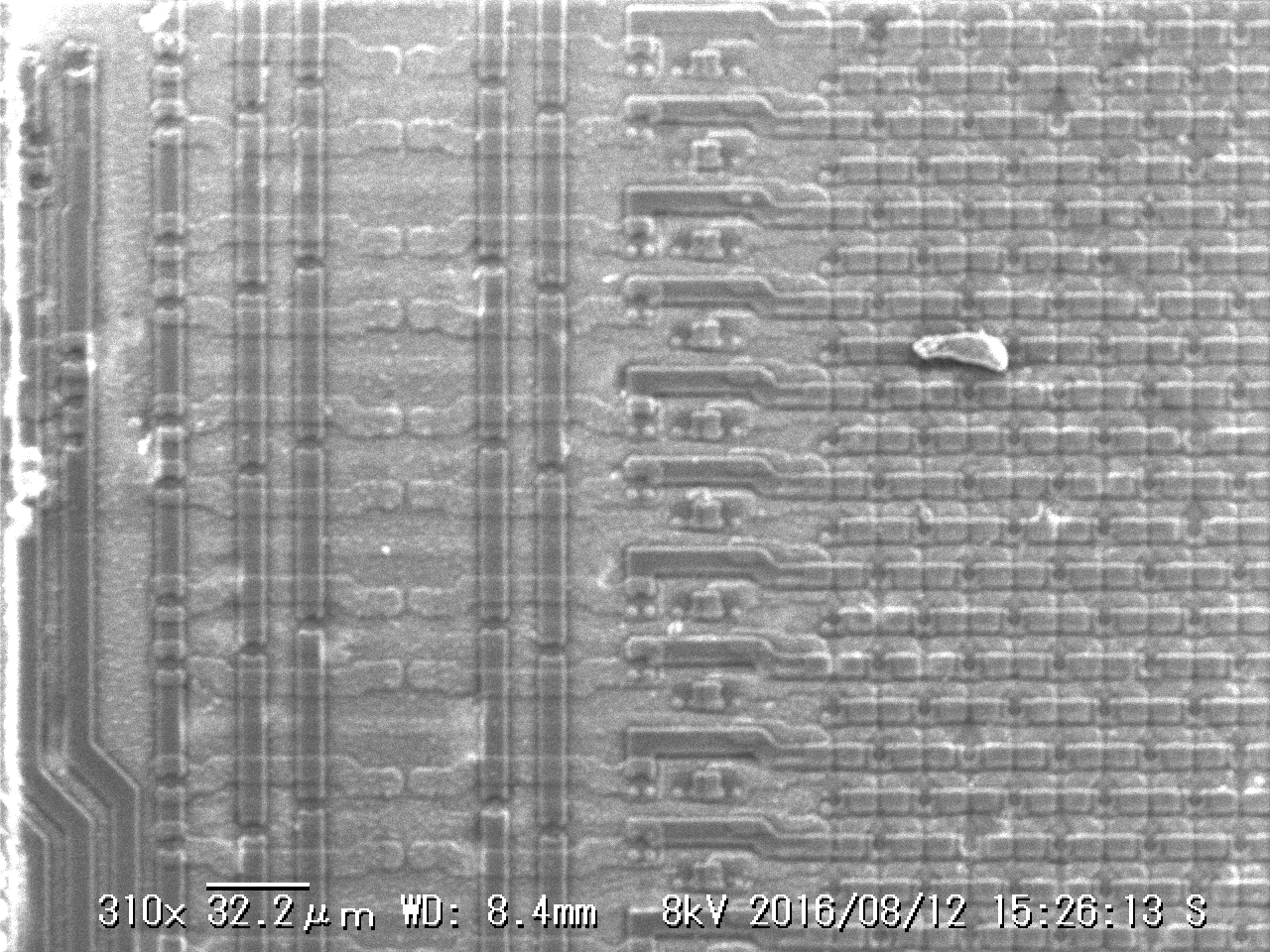
Some more random shots showing the bonding pads, you can see there’s a bunch of (I guess addressing) logic around the pads and next to the ROM matrix:

20160812_145454.bmp

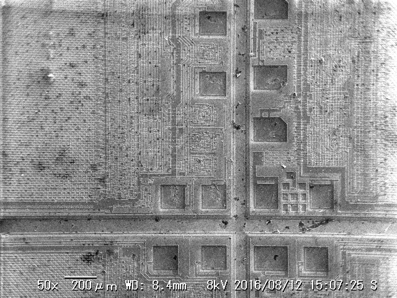
The corner where 4 dies meet, I just thought it looked kind of neat:

20160812_150725.bmp

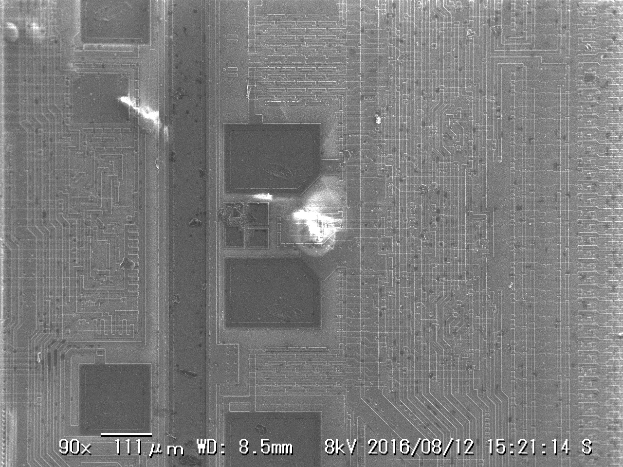
Enhance:

20160812_152114.bmpEnhance:

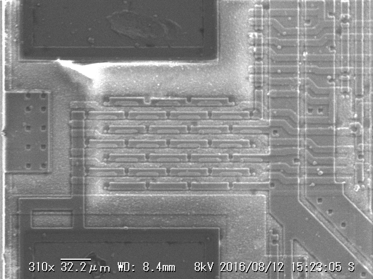
20160812_152305.bmp

Track right, enhance 224 to 176:

20160812_152440.bmpTrack 45 right:

20160812_152613.bmp

I wanted to focus in on one feature, even if it was just random junk on the die and see what kind of resolution I could get.

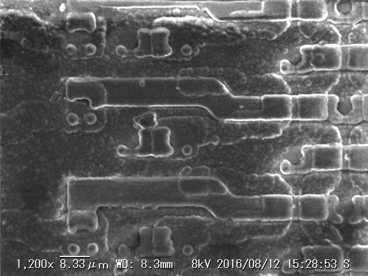
Enhance 34 to 46:

20160812_152853.bmp

Following images look further at the structures to the far right of the image.

57,19. Things look so messy up close:

20160812_153853.bmp

Hmm not very interesting:

20160812_154137.bmp

I picked this random blob and zoomed in further. I assume these is just a random fabrication defect:

20160812_153710.bmp

15 to 24 Give me a hard copy right there:

20160812_153456.bmp

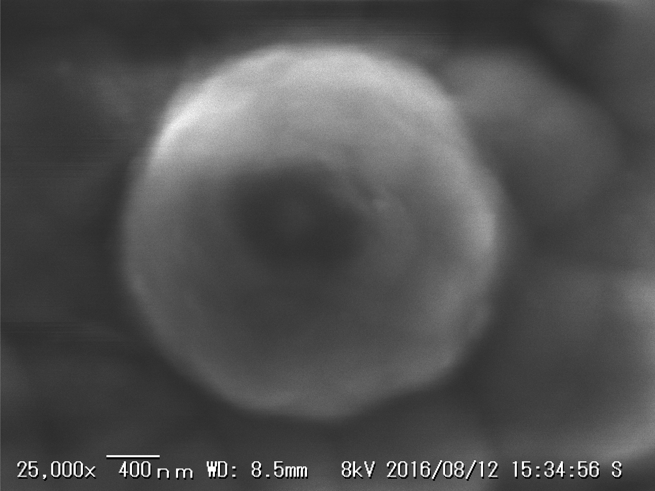
That’s a big/small blob of something! But at least we’re at the nanometer scale now. Anyway there we go. Suggestions on things to throw in the SEM? let me know!


Ugly Solutions

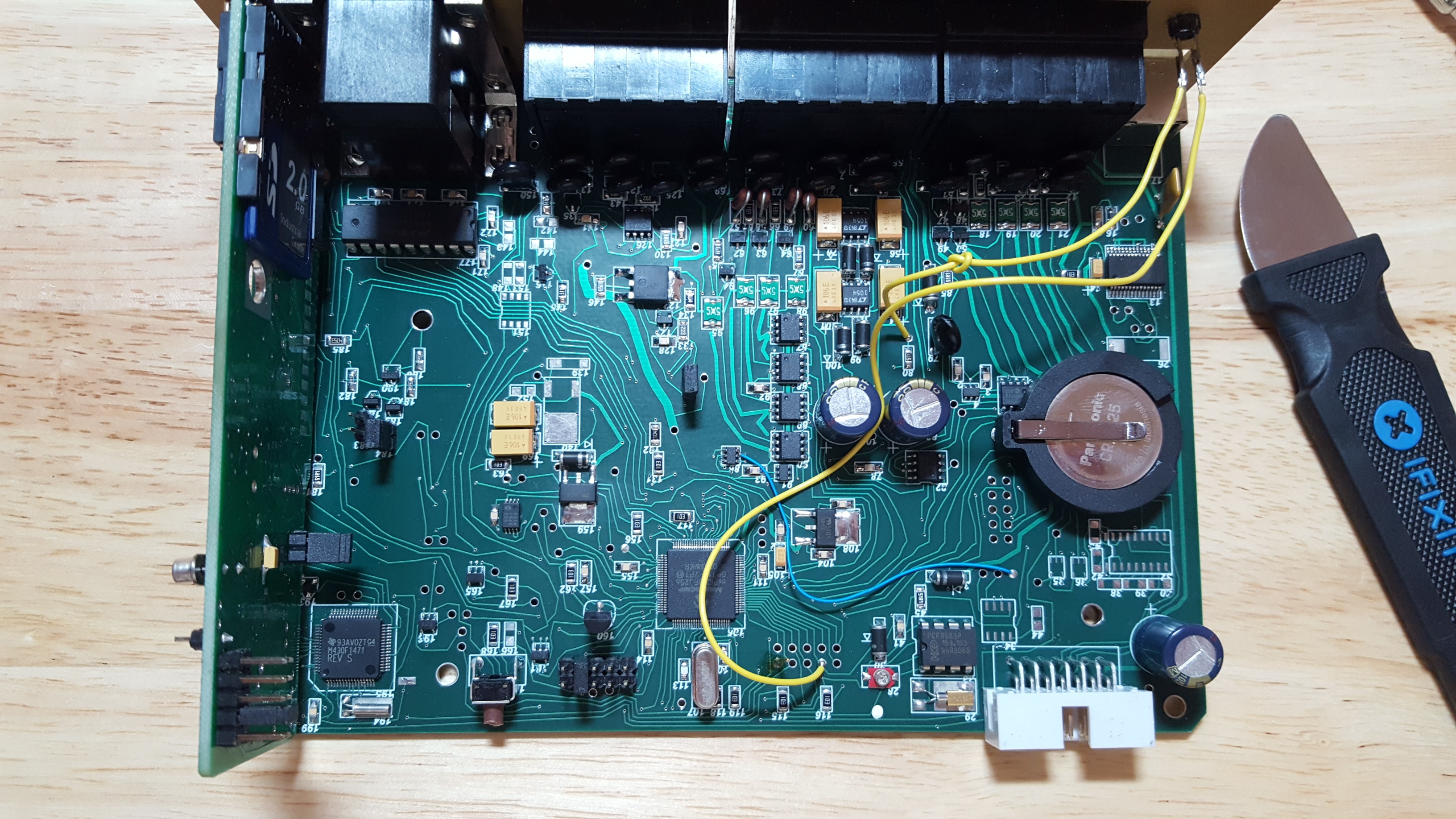
pcb1

The above PCB was posted on twitter a couple of days ago. Along with the comment “when PCB design goes wrong”. @whitequark mentioned topological router TopoR this was a new tool to me, but produces similarly non-traditional layouts. But this particular board doesn’t really look like the traces are following any kind of shortest path. It looks more like someone went a bit wild with the routing tool. I find this, overall, to be a pretty ugly PCB. But then I got to thinking…

The traces that spring out at all kind of angles are no doubt “inefficient” and I can’t really find any reason to suggest this is layout style is a good idea. But then I went and looked at the vendors website. The staff list is really interesting too. They’re clearly a medium sized business supplying real and effective solutions. These kinds of businesses are pretty though, there’s no pile of VC money to burn through and “move fast and break things”. It’s podding forward, providing real solutions. I’d also guess that, like most real businesses, it’s not about the quality of the engineering solution. It’s about meeting customer requirements.

And at the end of the day if the product was delivered on time, and met the customer requirements that’s all that mattered. In particular, there’s no EE listed on their staff page… perhaps the solution sub-contracted and this was what was delivered. It met spec and so it shipped. That was probably the right call, because if you can’t solve customer problems you don’t get paid and your staff don’t get paid.

So while the (poor) engineer in me wants to say this is an ugly board, who am I to judge.

There’s one other point to make, you might think you build a better design. But I’d almost guarantee that if you did you’d get zero sales. Everything around this board, the marketing, the integration, the customer support, matters more than the design itself. And that’s probably why they have a successful business.

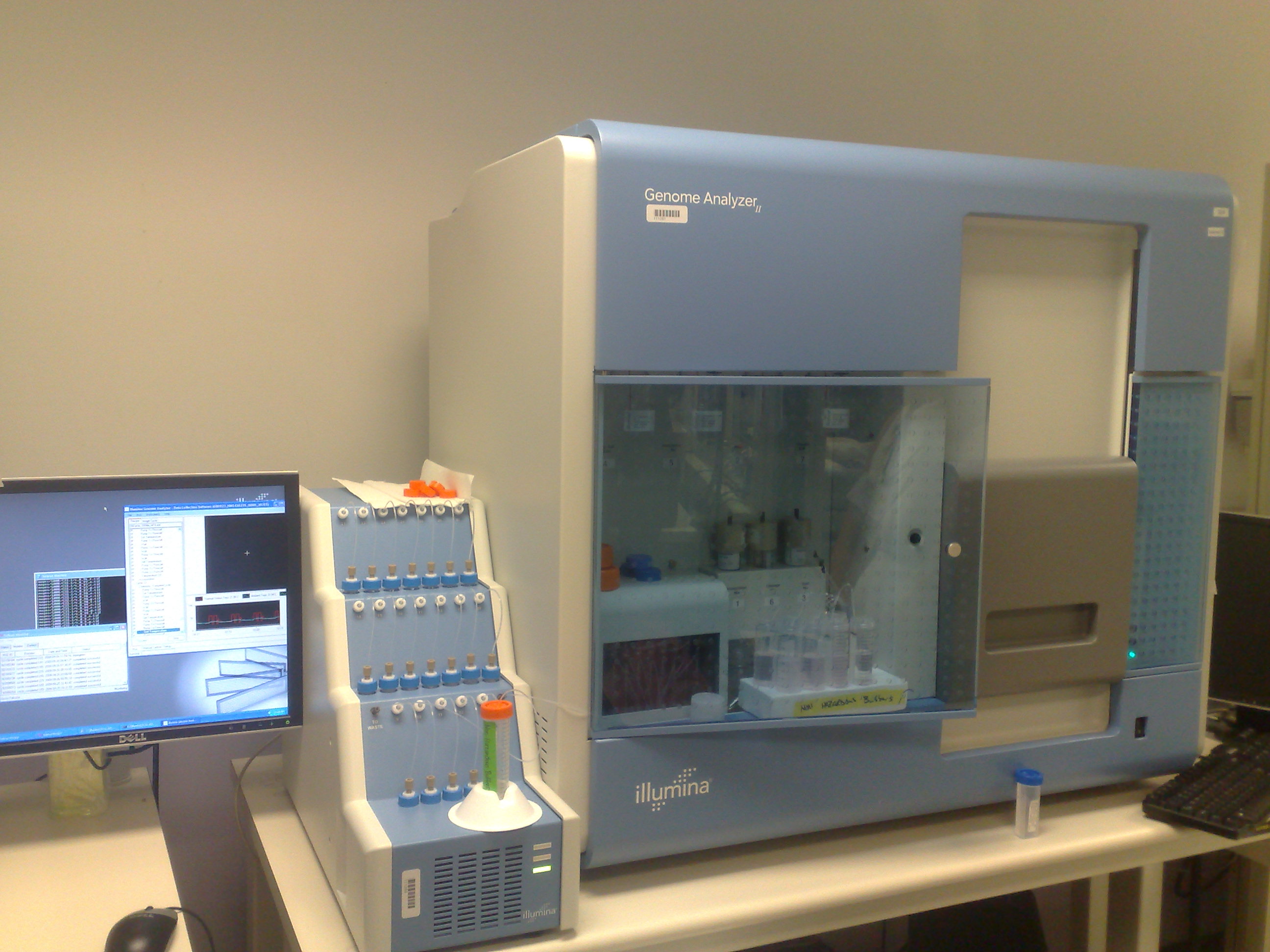
Illumina_Genome_Analyzer_II_SystemI wanted to share one more example. The instrument pictured to the right is an Illumina/Solexa Genome Analyzer II. The first of the current generation of DNA sequencers. If I remember correctly they cost about 250,000USD. I have fond (?) memories of this machine as a I wrote a bunch of analysis code for the raw image data they generated… But that’s not important.

Now, you might think that inside this machine you’d find a beautiful engineered solution worth the price of a good sized house in most parts of the world.

You’d be wrong.


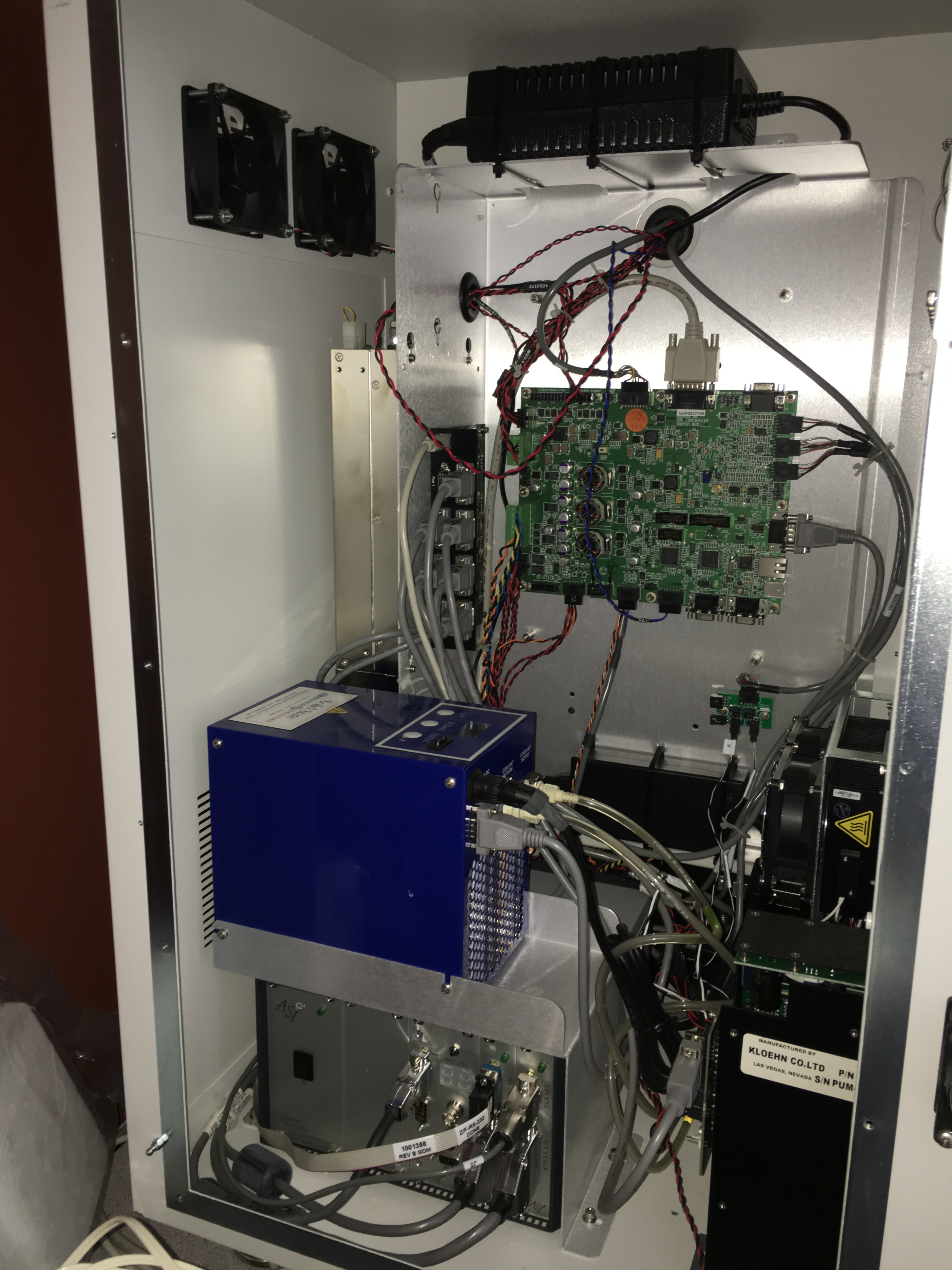
illumina_ga2To left is the engineering solution you’d have been buying. There’s a pretty big custom main control board in the middle (using IIRC an STM32). Just to the left of it you’ll see a bank of DB9 connectors. Those 7 cables are all RS232 ports. On one end they go to various pieces of lab equipment housed inside the case, on the other a USB RS323 adapter which heads over to a Windows PC for device control.

No custom laser drivers, integrated OEM stepper control boards.. just a big pile of rack mount lab equipment thrown in a box and some cable ties.

Pretty much everything is running off mains voltage. There are at least 4 power bricks which have been strapped into the case. I think there’s at least a couple more on the other side of the instrument. They’re probably all producing the same voltages…

Overall I consider this a pretty poorly integrated solution… but here’s the thing. Solexa the company that developed this instrument shipped it. They got their product to market and in a matter of months produced more DNA sequence data than had been sequenced since the discovery of DNA in the 1950s.

The engineering solution wasn’t the best, but the science was good, and time to market was more important that having a beautiful (or even cheaper or more reliable solution).

The AT24C01 and the AT24C01A

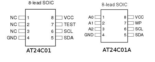
at24c01_at24c01aYesterday I was working on the mirror switch which is a network switch with static port mirroring config. This basically mirrors all traffic on one port to a second interface which lets you monitor and inspect traffic.

The switch loads config from a small EEPROM. The datasheet specifies a 24C01~16… I picked up some more AT24C32s which looked compatible with the AT24C01A and ordered a few AT24C01As… of course it didn’t work. Which led me down the rabbit hole.

These EEPROMs use a 2-wire protocol, basically serial clock and an I/O pin that switches between input and output based on the serial instruction. I spent some quality time with a scope trying to figure out why exactly the AT24C32 wasn’t working. It’s a 2-wire EEPROM in the same series… seemed like it should work.

After some head scratching I looked again at the datasheet. It specifies a 24C01… no A… The AT24C01 has long been deprecated by Atmel. But looking at the parts the AT24C01 and AT24C01A seem similar… largely compatible pinouts (just some added address lines)… they have the same function…

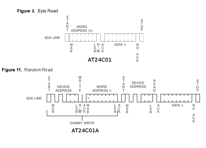
at24c01_va_protocol

Protocol differences between the at24c01 and at24c01a

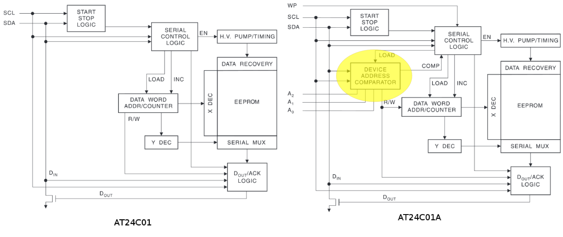
at24c01_va

Differences in the block diagrams..

But the protocol is different. Somewhere between the AT24C01 and AT24C01A Atmel decided that they needed per device addressing. Each command sent to the device therefore includes the device address, making the part non-backward compatible.

What’s interesting is that AT24C01 style parts are still being used in current generation products in Shenzhen. You can find knockoff AT24 C01s as jellybean parts on taobao. My guess is that somewhere around the release of the AT24C01 the ecosystem decided to standardize on this for a bunch of products and that was that.

Outside of Shenzhen things moved on, while Microchip has a great compatibility chart showing common devices compatible with the AT24C01, almost none are available (in fact many of the companies they mention don’t even exist anymore). There’s a single part on digikey which looks like it should be compatible… the 24AA01. Which is on it’s way to me… I live in hope (UPDATE: neither the 24AA01-I/SN-ND or 14C01BT-I/SNCT-ND which I purchased from digikey appear to be compatible despite the compatibility matrix saying they are, closer inspection of the datasheet kind of implies this, I’m working on another solution).

What’s interesting to me is that all this is probably common knowledge in Shenzhen, and a 5min chat at a EEPROM booth would probably reveal all… but for me it’s half a day of debugging. 🙂

The esp8266 and SD Cards

espusb1espusb2Recently I’ve been using the esp8266 with SD cards in order to develop the small board shown above and to the right. It hosts a CH340g USB interface, small buck converter to supply 3.3v to the esp8266 and an SD card slot.

The esp8266 is pretty thin, and doesn’t really give the information necessary to get up and running, so it took some research and hacking around to get everything working.

A lot of this was motivated by this forum thread which provided that it was possible to get SD cards working on the esp8266 using the SPI interface. SD cards generally use a more complex protocol and multiple data lines, but they can fall back to SPI mode (albeit with reduced performance).

The Arduino esp8266 support pack also has done great work, and after configuring a chip select pin, the SD card library supplied there pretty much just works.

I wanted to use the native esp8266 SDK without the Arduino environment. This took some hacking, but so far I’ve extracted the SD card library and have it up and running using a native SPI driver, the main issue was enabling (the again undocumented) duplex mode of the esp8266 SPI interface. If you’d like a copy of this code ping me.

One final note, some documents refer to “SD Card” boot mode. That would be really cool, to be able to load your firmware directly from an SD Card. Unfortunately it’s a bit of a misnomer. “SD Card” mode actually refers to SDIO mode. We don’t really hear much about SDIO anymore, but you used to be able to buy these funky Wifi cards which plugged into SD card slots. Other peripherals, like cameras were available too. You can read more about it on the wikipedia page.

The esp8266 supports an SDIO boot mode. My guess is that this is a hang over from its heritage as a general purpose Wifi interface chip. Some people have used this functionality to enable firmware loading over SPI. It’s neat, but unfortunately doesn’t mean you can boot from a standard flash SD card.

PLUG: I’m now selling the esp8266 SD card board above on my shop. My hope is to eventually progress this toward a consumer product which runs an access point and provides basic collaboration tools.