Random SEM Images – MCM68364 64KB ROM
I wanted to make sure the SEM was still happily chugging away so picked up some cheap wafer fragments on eBay and did some imaging. Truth be told, I think I just enjoy throwing things in the SEM and seeing what they look like. If you have something you’d like imaged drop me a line (particularly if you’re from the hacker or maker community) and we can arrange to have it imaged. Currently samples need to be conductive as we don’t have a sputtering machine up and running here yet.
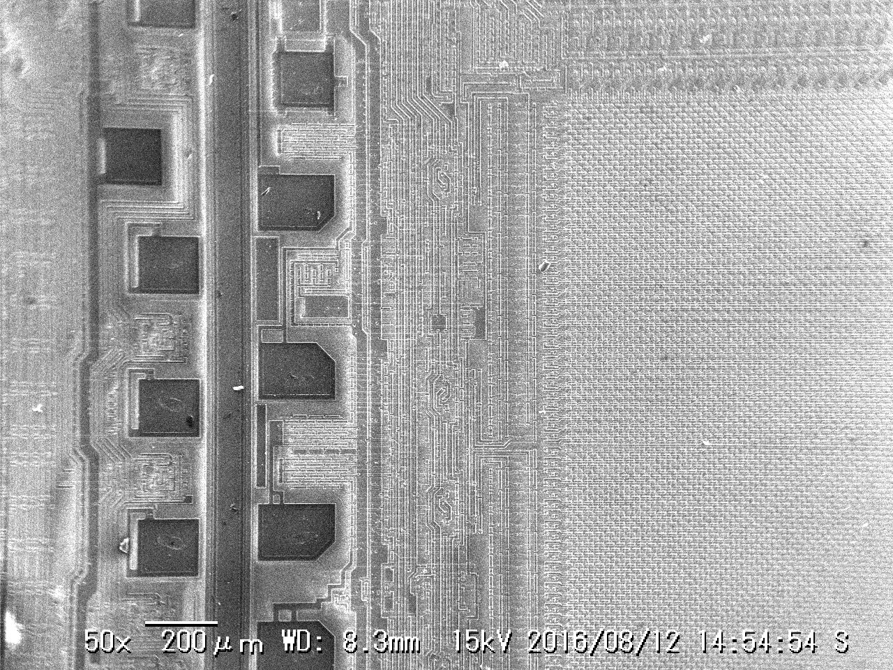
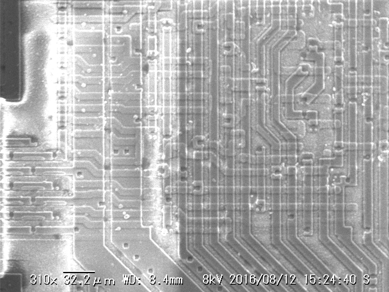
Anyway… on to the images! Here’s a shot at the lowest magnification:
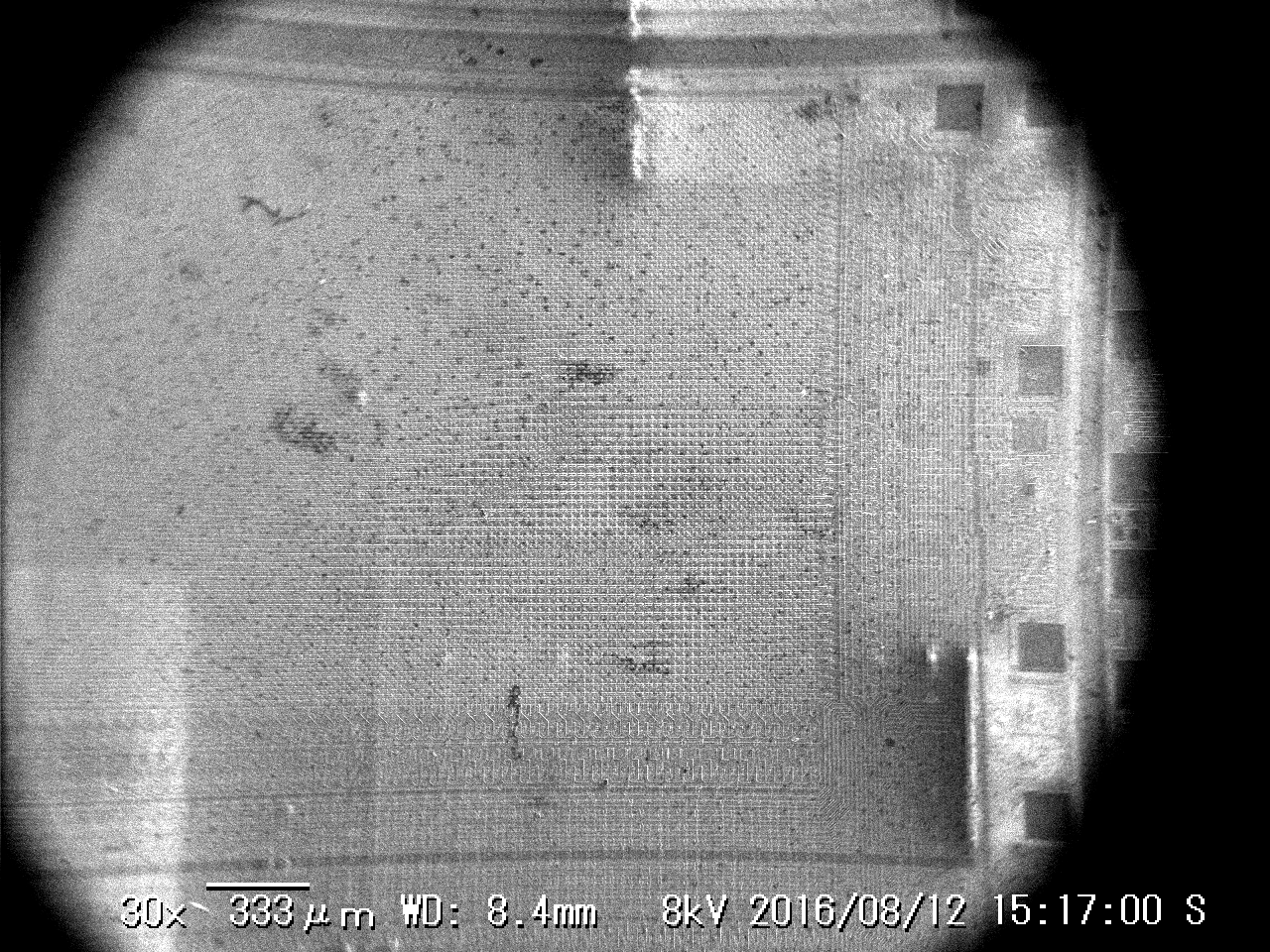 Honestly, it would probably just be better to use an optical microscope here. And in fact, the features on this chip are relatively big. But I do love the fact that with a SEM you can go all the way from 30x to 20000x.
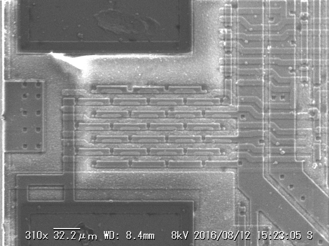
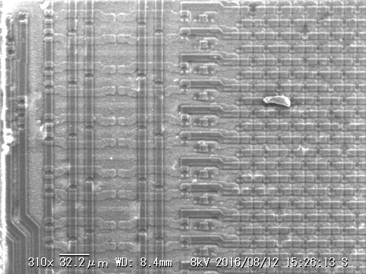
Here’s a random shot of part of the matrix, I’d guess this is something like a 1 micron process? Maybe sub-micron but not double digit nanometer. Pretty old stuff:
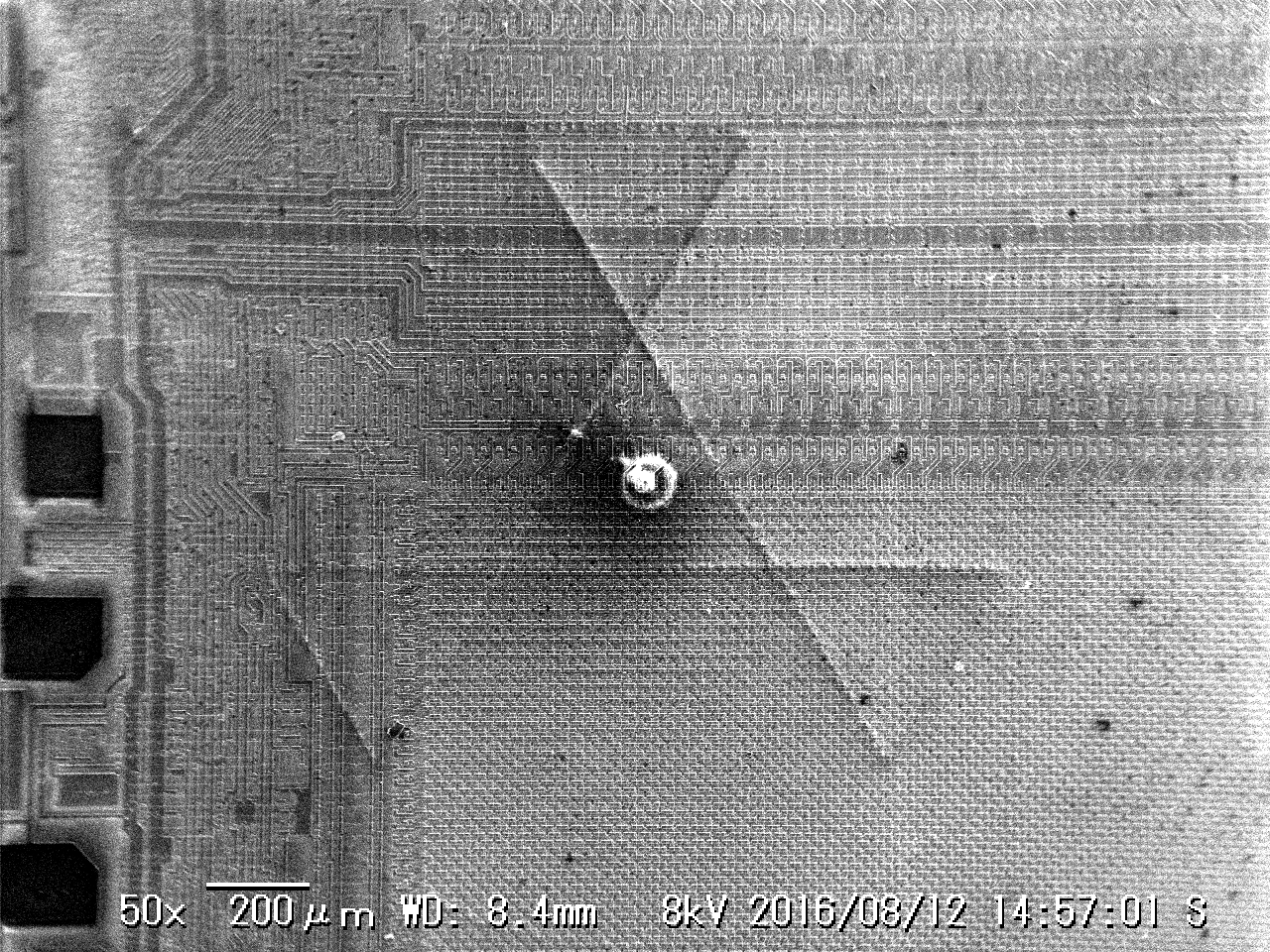
After taking that image I zoomed out a bit. Thing about SEMs is that they’re often somewhat destructive. You can see that the die has been scared in that area. After that shot I lowered the acceleration voltage a bit…
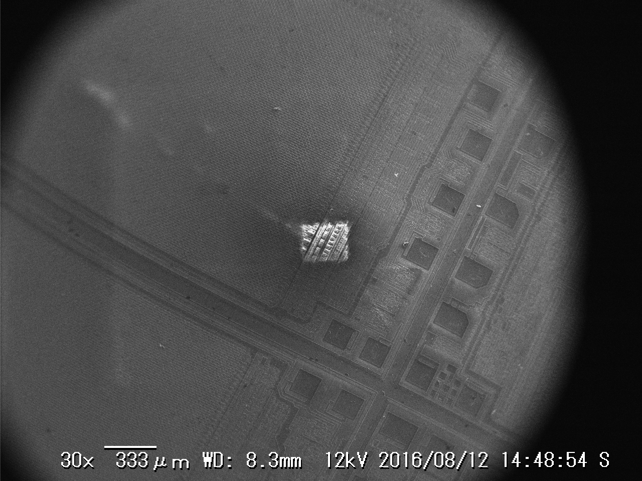
I’m guessing there’s a reason these wafers found their way onto eBay and not into a product.I assume this marking was produced by test jig to mark dies as faulty:
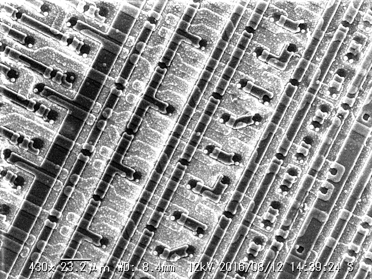
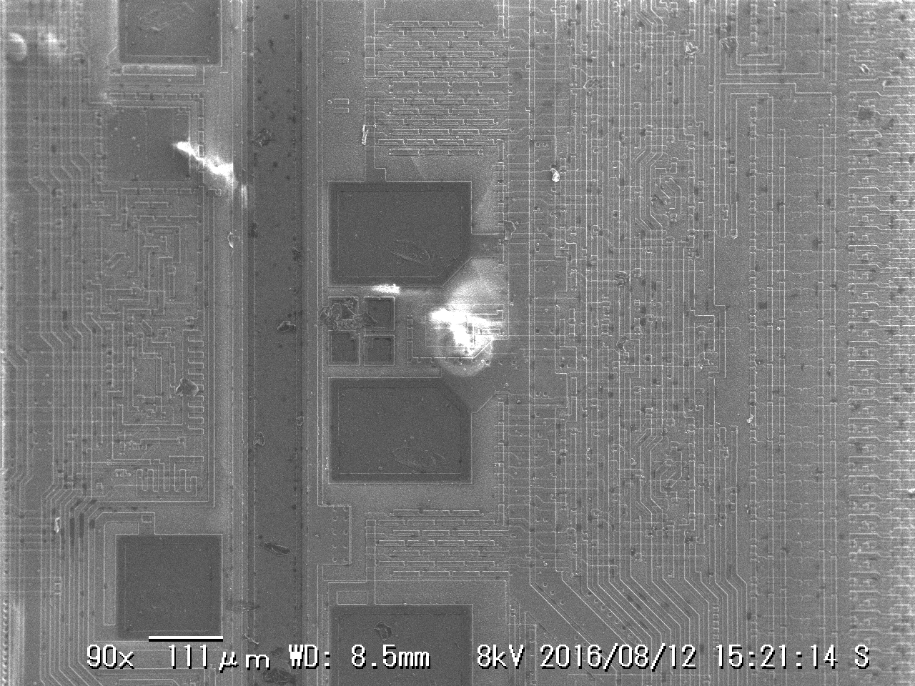
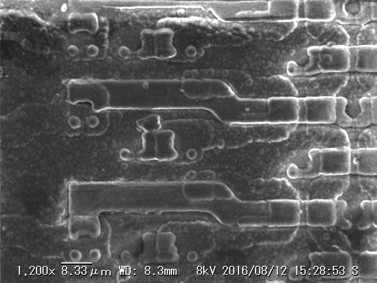
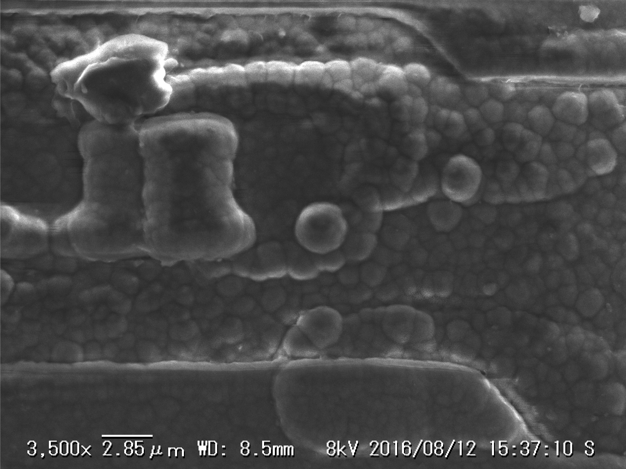
Some more random shots showing the bonding pads, you can see there’s a bunch of (I guess addressing) logic around the pads and next to the ROM matrix:
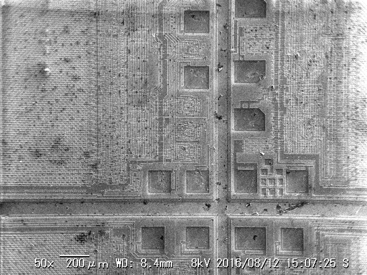
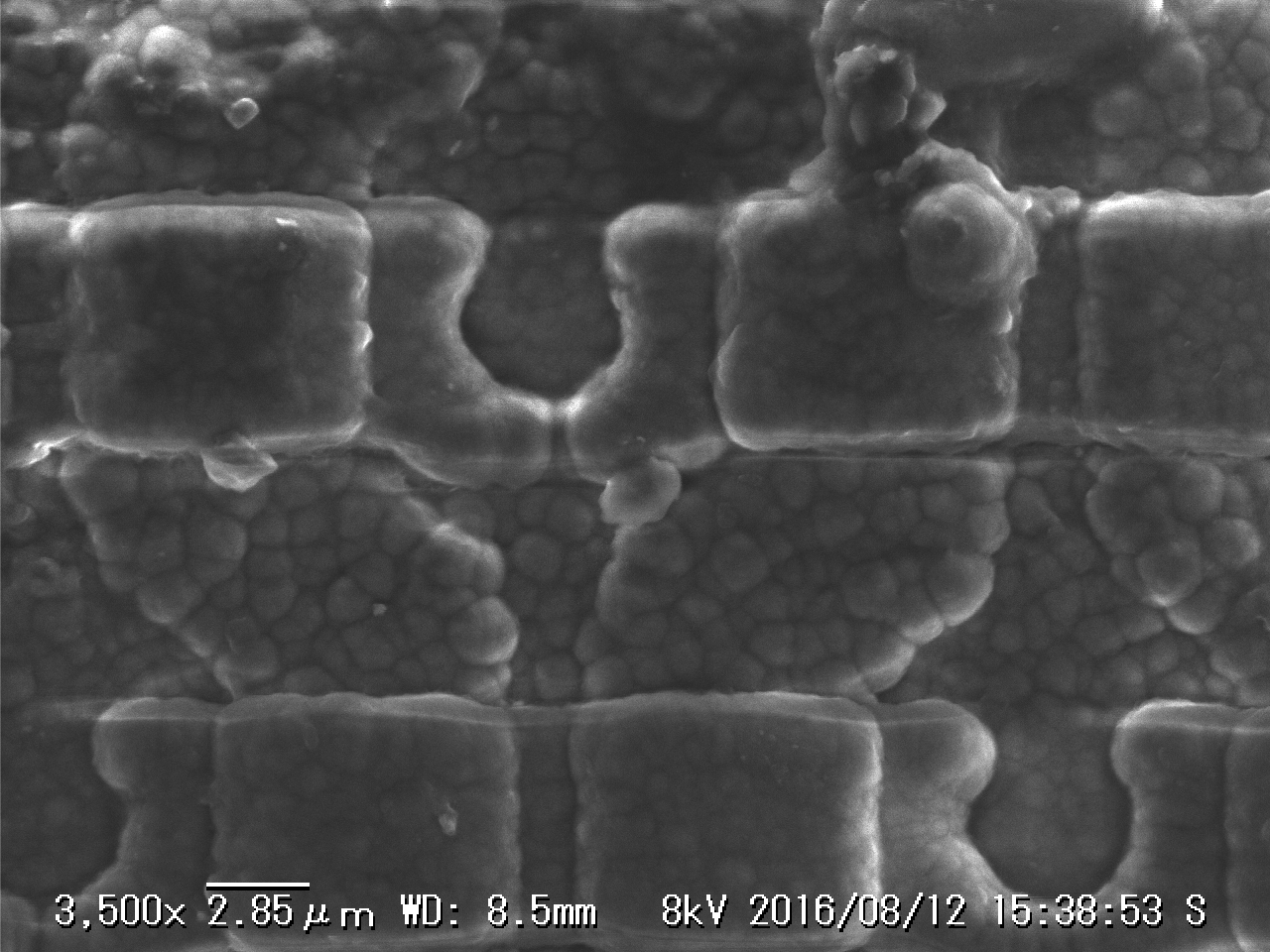
The corner where 4 dies meet, I just thought it looked kind of neat:
Enhance:
 Enhance:
Track right, enhance 224 to 176:
 Track 45 right:
I wanted to focus in on one feature, even if it was just random junk on the die and see what kind of resolution I could get.
Enhance 34 to 46:
Following images look further at the structures to the far right of the image.
57,19. Things look so messy up close:
Hmm not very interesting:
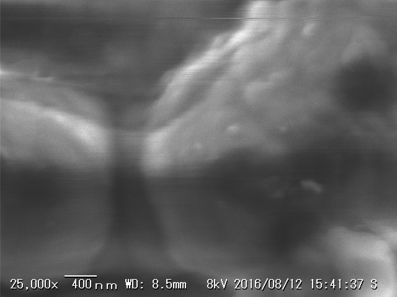
I picked this random blob and zoomed in further. I assume these is just a random fabrication defect:
15 to 24 Give me a hard copy right there:
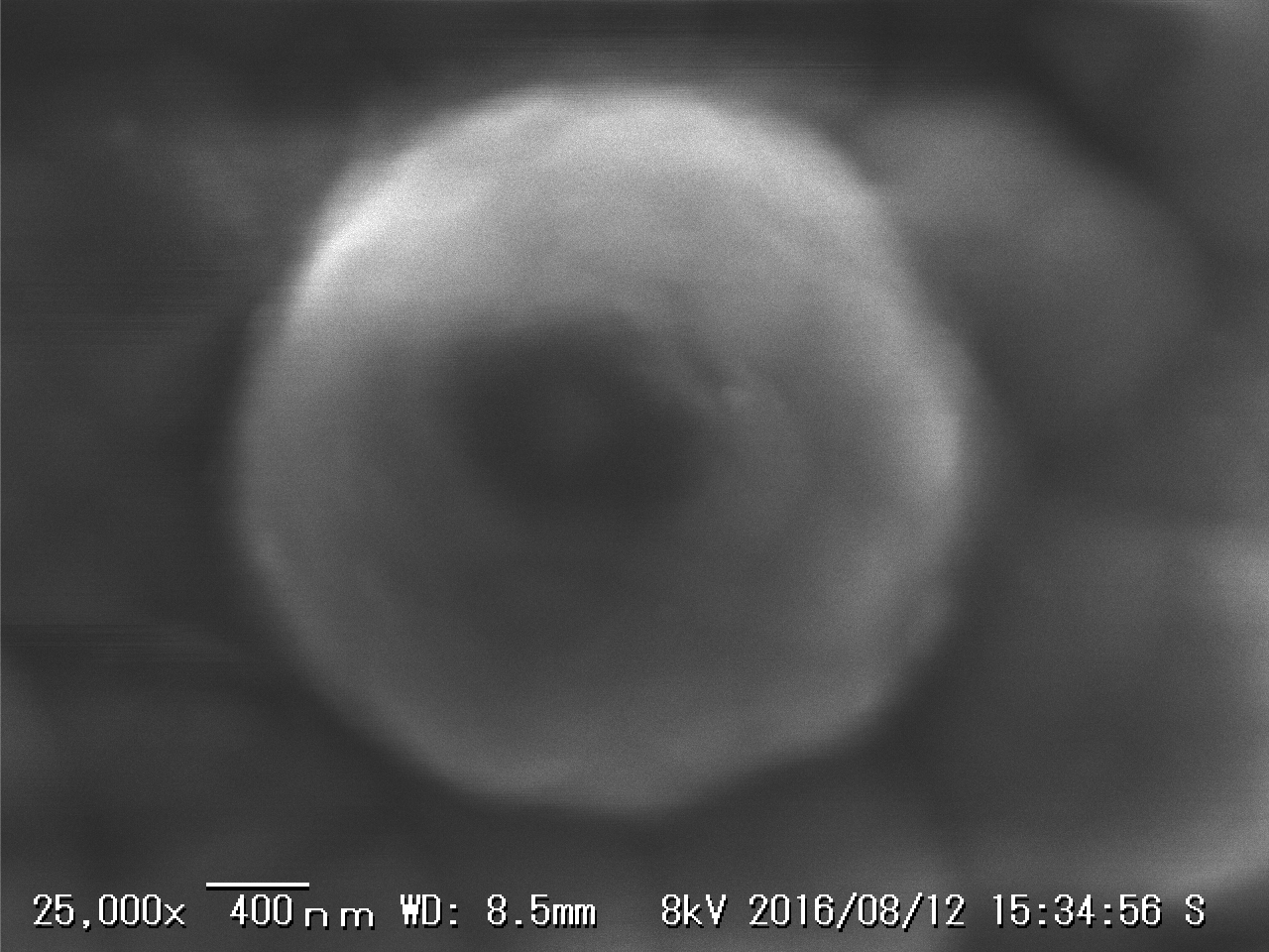
That’s a big/small blob of something! But at least we’re at the nanometer scale now. Anyway there we go. Suggestions on things to throw in the SEM? let me know!
http://guessthissem.tumblr.com
Yea those Keyence SEMs are seriously easily to use. We didn’t even use the English manual in the end. I’m impressed you’re getting such good results without (I assume) sputtering non-conductive samples. Hope all is well!