Speculation on the Illumina FireFly

Keith over at OmicsOmics has an interesting write up on the recently announced Illumina Firefly system. As always, his views are interesting and informative, however he makes one assumption that I think may not be entirely warranted:
“The name is fun, though a bit curious given that the goal is to not use any light”
Here’s what I know about Firefly, which all comes from GenomeWeb via OmicsOmics:
- Uses a one-channel version of SBS chemistry.
- Based off CMOS sensor technology that Illumina acquired when it bought Avantome.
- Commercialize in second half of 2017.
- Costs <$30,000, cost per sample ~$100
- Library prep module uses digital fluidics, can process 8 samples in parallel.
- 1.2 gigabase per run.
- Uses nanowells that enable patterned clusters of DNA deposition.
From this I infer the following:
- It’s not a single molecule approach (note clusters).
- The chemistry is similar to their current chemistry.
- Uses a sensor that detects a single intensity type (i.e. no active filters, or differing illumination).
- Sequencing happens on a semiconductor somehow.
- May or may not have something to do with Avantome.
The pricing, cost per sample, and release data doesn’t express much about the basic technology. They are purely based on market factors. As is the current Illumina pricing.
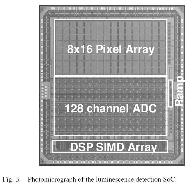
Chip structure from the IEEE paper.
My initial guess based on the above data was that it’s an optical approach, using the existing chemistry on an integrated silicon “lab-on-a-chip” style sequencer. So I had a look around, first thing to do is a patent search. I couldn’t find anything directly relevant. But a bunch of their patents contain the following boilerplate statement:
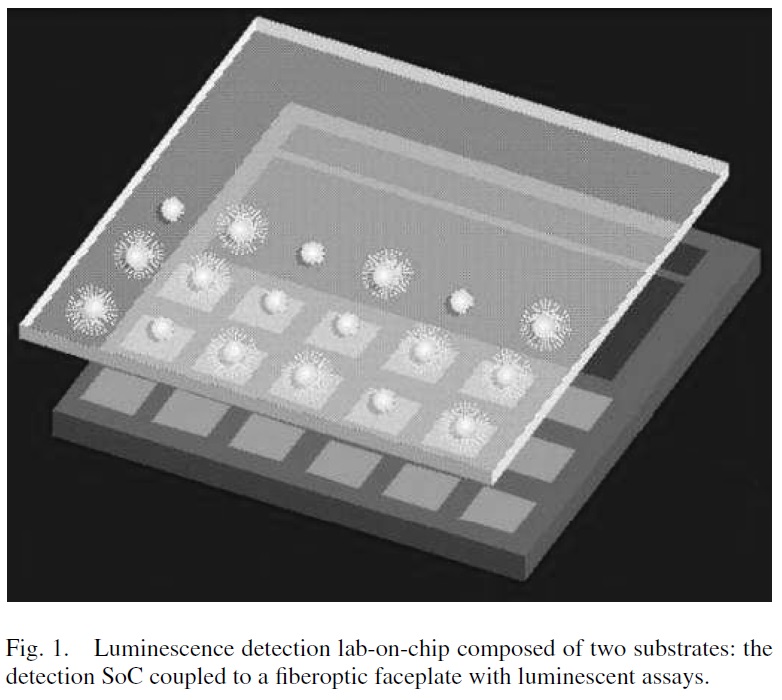
In some embodiments described herein, detection of the signal, such as light emitted form conversion of ATP and luciferin, or light emitted form a fluorescent label, is detected using a charge coupled device (CCD) camera. In other embodiments, a CMOS detector is used. Detection can occur on a CMOS array as described, for example, in Agah et al., “A High-Resolution Low-Power Oversampling ADC with Extended-Range for Bio-Sensor Arrays”, IEEE Symposium 244-245 (2007) and Eltoukhy et al., “A 0.18mm CMOS bioluminescence detection lab-on-chip”, IEEE Journal of Solid-State Circuits 41: 651-662 (2006).
TL;DR: We can use a CCD camera (like current instruments) or we might use this thing talked about in the paper they reference. Here’s part of the abstract:
The paper describes a bioluminescence detection lab-on-chip consisting of a fiber-optic faceplate with immobilized luminescent reporters/probes that is directly coupled to an optical detection and processing CMOS system-on-chip (SoC) fabricated in a 0.18um process. The lab-on-chip is customized for such applications as determining gene expression using reporter gene assays, determining intracellular ATP, and sequencing DNA…
 There also a nice presentation with the same title here. So what happened to the authors of the paper? Well the paper thanks Mostafa Ronaghi (current Illumina CTO via Avantome and NextBio). And its first author is Helmy Eltoukhy. His LinkedIn profile says he went on to become President and CEO of Avantome, before joining Illumina working on “Semiconductor-based Genetic Analysis Systems”.
Of itself I think this is enough to suggest that they’re looking at a photonics based lab-on-a-chip system using labels likely based around Bioluminescence.
I also came across this old job advert for a “Staff Development Engineer – Silicon Nanophotonics at Illumina” requirements include:
- Deep understanding of near field optics, physical principle of micrometer and nanometer scale silicon photonic devices
- Solid understanding of CMOS devices and semiconductor fabrication processes
- Experience with MEMS, biomedical equipment & devices, lab-on-chip
Finally, as I briefly mentioned above, those chips don’t use fluorescence like current systems. They use bioluminescence… you know… like fireflies… Hmmm? Get it?
 Now onto some more speculation…
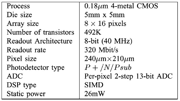
The analog and mixed signal circuitry, seems very similar to what you’d find in the photo-diode array industry. In a CCD, there’s typically a single amplifier and ADC, which is used to read out all the pixels. Photodiode array chips however often have an amplifier and ADC per sensor. You can typically find 128 channel integrated acquisition chips like the DDC1128. They operate at a few KHz bandwidth though and are used in things like CT scanners. The paper suggests they have a higher bandwidth. I’m not sure why this is necessary (see the table), but is seems kind of fun!
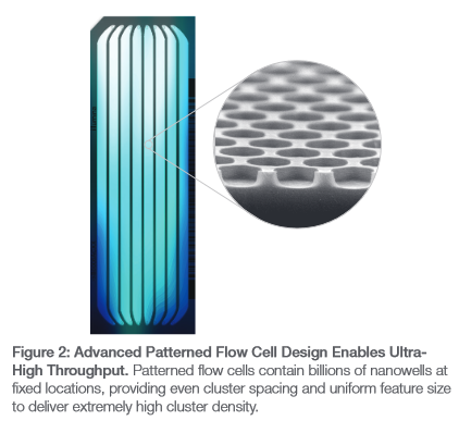
They use a patterned flowcell like their current instruments. Patterned flowcells no doubt simplified primary data analysis massively. In my experience, image analysis was always the most costly part of the primary data analysis process. Patterned flowcells should have made it much easier to extract intensities from clusters. The sensor per cluster approach simplifies data analysis by another order of magnitude, throwing out image analysis completely and allowing basecalling to from intensities directly.
And the basecalling process itself should be much simpler. There’s no crosstalk between lasers to compensate for, unless there are new signal artifacts your really just left with phasing to correct for. How much compute you require will depend on how many sensors you have. Let’s try and run the numbers.
We know the output is 1.2Gbases per run. Illumina read length tops out at 2x300bp. 1.2Gb/300/2=2 million. So if the above makes sense, we’re looking at a 2 million sensor chip. I have no reason to believe that isn’t feasible. From the IEEE paper, it looks like the pixels and acquisition electronics take up about equal space, so in terms of real-estate this is similar to a 4megapixel CCD. They might however be doing the acquisition differently. Making the die smaller than this.
So the chip needs to be as big as the flowcell. It would be interesting to know how big the die needs to be to accommodate 2 million nanowells and if this a sensible number.
You can probably work out the nanowell size from the number of reads per lane and size lane size. The illumina spec sheet contains the figure to the right which shows a SEM image, but no units.
You have to be careful with pdfs though, as they can contain vector graphic as well as bitmap data. And vector graphics… over bitmap data. Google indexes all the images in the pdf even if they’re not visible.
Turns out that clipped SEM image is just masked in the pdf. Here’s the full SEM image which helpfully shows us the scale:
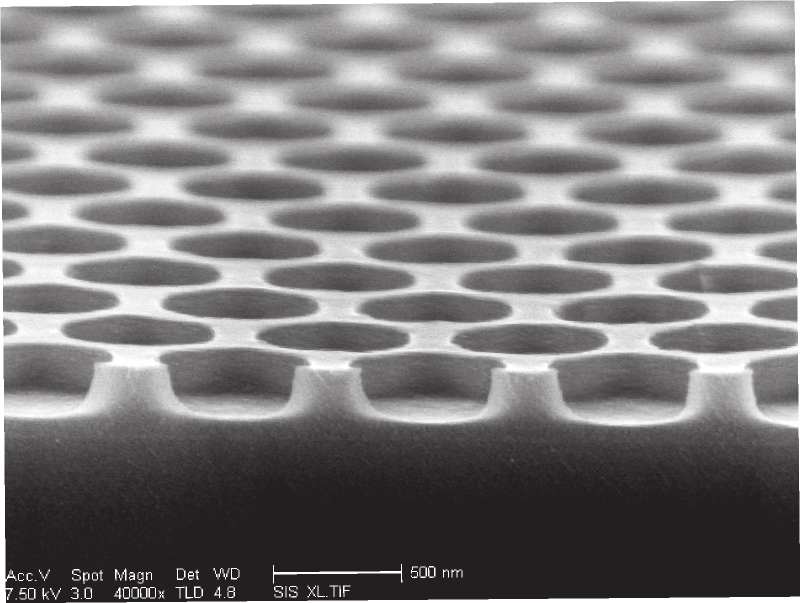
So a reasonable guesstimate is that the current wells are 500nm in diameter. Some futzing around on packomania tells me I can pack about 110 500nm circles into a 5000nm square. So I’ll need about 18181 of those squares, or 670 microns. A tiny about of space. I’d guess they’ll need more space than that, but the message is I can’t see the well size being a limiting factor.
Lets run the numbers again using the pixel size from the paper (240microns). If that were the case you’d need something like a 339mm squared die. Way too big. Those are pretty huge pixels though. For a reasonable sized die they must be using something much smaller. A pixel size of 10microns or smaller would be feasible I think, these are common in CCD cameras. The smaller the die, the cheaper. It’s unclear if the die is a consumable or not, but it’s certainly a possibility.
A 2 million sensor chip therefore looks like a reasonable guess. For my prior experience writing Illumina basecallers, basecalling 2 million intensities should be quite feasible on a low power processor, similar to what you’d find in a mobile phone.
So this is what I suspect we’re looking at, a small bioluminescence semiconductor sequencing platform which could potentially be very cheap. I may ponder a little more on what a single channel chemistry looks like, and the overall system architecture.
If the above is correct it’s a solid, iterative move development which is characteristic of Illumina. Illumina’s execution has always been excellent (and by excellent I mean better than everyone else). They’ve also always incrementally improved on their existing platforms, introducing chemistry improvements, new flowcells, and better acquisiton systems, slowly. This is also an incremental improvement in many ways. It retains all of their developments in chemistry but introduces a new labeling scheme and on die readout.
It is likely to enable them to produce a drastically cheaper sequencing platform, if they choose to go that route. However I don’t think it will enable massively longer read lengths. It may also prove difficult to scale the platform much beyond a few Gigabases and they are currently limited to a single read per well.
Disclaimer: I have to finish up with a disclaimer. I have stock in sequencing companies. I’ve worked for sequencing companies. This post is based on the information I’ve been able to dig up publicly (and is all I know that’s relevant anyway). This is all speculation, though I’ve tried to assess the technology on its merits.
I’ve found some better images of the patterned flowcells, which have a visible scale, over at coregenomes: http://core-genomics.blogspot.co.uk/2016/01/almost-everything-you-wanted-to-know.html
I guess they come from Illumina literature, and that’s generally public info. I still enjoyed hacking apart the pdf though.