Notes on the Keithley 2002 ADC
The Keithley 2002 is an 8.5 digit multimeter. This puts it among the highest precision multimeters available. I’ve been curious about the ADCs used in these high end multimeters and have been looking over the Keithley 2002 ADC schematic. These are my notes.
The schematic I used is from TiN. Originally this was hosted here but appears to currently be offline. A local copy of the schematic is here.
As far as I can understand the ADC is a dual slope implementation (UPDATE: it’s actually multislope, but the slow slope is always connected, see below). The slopes are driven by current sources of ~450uA (which are derived from a 7V reference). They are switched through a SD5400, and when not in use flow to some kind of current sink.
I’ve mostly looked at the current sources, and switching. As part of this, I’ve been playing with an LTSPICE simulation (download):
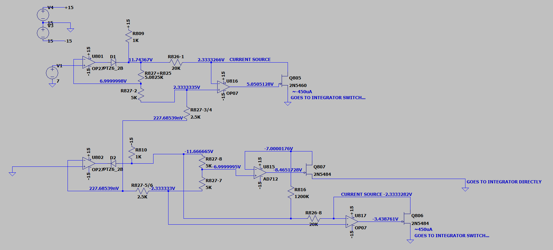
The Keithley 2002 uses a 7V LTZ1000 reference (generally regarded as the best voltage reference you can buy). This enters the ADC board as a differential signal (REFHI and REFLO). REFHI should be 7V and REFLO ~GND. The REFHI is used to feed a non-inverting opamp (U801). The opamp has gain of 1.666. A tap is taken off the feedback network of U801 at ~2.333V. This is used as the reference for U816. This opamp drives a JFET (Q805) such that 2.333V flows through it. Creating a current source. Setting the voltage through Q805 seems to set the current at ~-450uA.
Rather than being ground referenced, the feedback network of U801 is connected to the virtual ground of U802. U802 is referenced to REFLO. U802 is an inverting opamp. Again with a gain of 1.666. Again a tap is taken off the feedback network at ~-2.333V. This is used as the reference for a opamp driving a current source created by Q806 (similar to the above). Current though Q806 is ~450uA.
The above therefore creates positive and negative current sources of +/- 450uA. These are the run down slopes of this dual slope implementation.
There’s another current source, Q807. This goes directly to the integrator. I don’t understand it’s purpose…
UPDATE: Kleinstein on the EEVBlog forums pointed out that there is a single slower slope which is always connected, delivering ~5uA. I assume this is what U815/Q807 are. So this is in fact a multislope ADC, but the slow slope is always connected.
The references are switched through an SD5400. These are MOSFET switches. The Vgs threshold is ~0.1V. It is driven by TTL logic level signals (0,5V). This being the case, if the voltage coming from the current sources goes below -0.1V or above 5V it will not switch correctly. Because the current is so low (450uA), a load of >200Ohms would be required to generate a voltage higher than 0.1V. I assume that the integrator presents as a load lower than this.
When not in uses, both the input and the references switch to a separate path, I’ve not looked at this path in detail. But kind of imagine this is used as a sink, which keeps the current flowing through the references constant…