Archive for September 2016

PIC Versus AVR

pic

As a general purpose microcontroller board I was always a bit disappointed with the Arduino. When in Arduino appeared in 2005 the 8bit AVRs were already pretty old school microcontrollers and cheap 32bit microcontrollers were already available. These days when you can pick up a cheap STM32 for under a dollar it seems kind fo crazy to use 8bit mid-90s technology…

The reason we do of course is because the Arduino has great support and a large active community.

For a recent project I wanted a small microcontroller. All it had to do was send a few very simple serial commands. For this, I really didn’t need anything more than an 8bit microcontroller, which for me comes down to PIC versus AVR.

I cut my teeth on PICs in the 90s using MPLAB under windows 3.11. PICs have a kind of nasty architecture. They’re Harvard architecture. Which means code and data sit in separate memory spaces, and that takes a little getting used to.

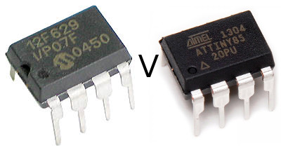
One of the nice things about PICs is that very have very very low power, cheap versions. The PIC12F629 has ~2KB of flash and 64 bytes of RAM. It’s about 1USD on digikey and about 10 cents on taobao. It also looks like there might be cheaper clones down to about 1 cent.

So I went with the PIC12F629 and it was a nightmare. Firstly, I thought I’d try using a C compiler, inefficient for sure but hopefully quicker than writing assembler. So I installed the debian package sdcc, which is the only compiler I know that supports PICs on Linux.

Debian sdcc doesn’t have PIC support.

sdcc uses the microchip header files which have a non-free license. It look me a while to figure this out but I then downloaded sdcc for their sourceforge site.

It’s a sourceforge site. I should probably have stopped right there. Binaries are available, but they are 32bit only. I checked out the source from their svn.

./configure;make;make install

Looks good. Could at least start to compile code, lots of issues. Size issues due to 32bit in library requirements (removed 32bit ints) etc. etc. Finally code looks like it should fit in the flash, but it’s failing to link with libsdcc.

Building sdcc doesn’t build libsdcc. Googling… digging around in random directories, and try and configure;make it. Fails. Missing instructions in the floating point library. Hack the floating point library until it builds…

Finally get a binary from sdcc.

I’m using a minipro to flash the controller. Fails.. the hex file is the wrong size.

The hex file contains a single word way off the end of the flash memory. This was actually the configuration bit, but the Linux minipro software doesn’t know how to flash this correctly. However with this removed the devices would flash and verify.

PIC does nothing when powered. Can’t even get an LED to blink.

I try reference hex files which should just blink LEDs… they don’t work.

I figure maybe the Linux minipro client doesn’t work well. So I try the Windows client. Many people have reported successes with minipro and the PIC (including the PIC12F629) so it should be an issue.

Fails.

Spend hours fiddling with config bits. Decoupling.. Power supplies..

Fails.

Give up, and buy a Digispark with a ATTINY85. Works within 5 minutes.

I’d literally spent hours with the PIC. I’m guess one possibility is that I’d overwritten the OSCVAL config in the PICs (which stores internal oscillator calibration) and the PIC was hosed because of this. But the conclusion is basically the same.

The AVR has a clean, open toolchain and a larger community, it’s just easier to get things done. At some point I’ll likely migrate my code to the ATTINY10 which are about the same price as the cheapest PICs (

Creating the miror swtich

FullSizeRender(8)

Since I last wrote about adding management features to a cheap 5 port switch I’ve been trying to productionize that work.

I wanted to load the switch with a static config, enabling port mirroring from ports 0 to 1 as a network diagnostics tool (plug: you can now buy this on my shop).

The ip178g can load its config from flash at boot, and the flash IC footprint is on the board. Great! Should be easily… well turns out not so much. The flash used is an AT24C01, this was superseded by the AT24C01A and is no longer available from the normal suppliers. I had a lot of fun figuring this out (and no they’re not compatible).

Ordering the part from Shenzhen would take a month, and because the AT24C01A is also thrown around prety freely I’m not confident that I’d get the right part anyway.

So, I decided to use an ATTINY85. Actually at first I decided to use a PIC12F629 (this was a horror story in itself). I purchased some digisparks and used code adapted from my previous post to send config messages to the IP178G. It would also be possible to simulate the the AT24C01, which might be an interesting project.

Before I gave up on the AT24C01 route I wrote a flash image builder. You can find this can the digispark code on github.

To mount the ATTINY85 in the switch I pulled it off the digispark and placed it on the AT24C01 footprint. For the most part the pins line up acceptably well. The ATTINY85 is a wider part, and a pullup resistor needs to be added to the reset pin, but this is an acceptable solution for now (the rework is shown above).

Digispark code is below for reference:

1
2
3
4
5
6
7
8
9
10
11
12
13
14
15
16
17
18
19
20
21
22
23
24
25
26
27
28
29
30
31
32
33
34
35
36
37
38
39
40
41
42
43
44
45
46
47
48
49
50
51
52
53
54
55
56
57
58
59
60
61
62
63
64
65
66
67
68
69
70
71
72
73
74
75
76
77
78
79
80
81
82
83
84
85
86
87
88
89
90
91
92
93
94
95
96
97
98
99
100
101
102
103
104
105
106
107
108
109
110
111
112
113
114
115
116
117
118
119
120
121
122
123
int clock_pin = 1;
int data_pin  = 0;
  
int width=100;
  
void setup() {
  pinMode(clock_pin, OUTPUT); // CLOCK
  pinMode( data_pin, OUTPUT); // DATA
}
  
int recv_one_bit() {
  int data=0;
  digitalWrite(clock_pin,0);
  delayMicroseconds(width);
  digitalWrite(clock_pin,1);
  delayMicroseconds(width/2);
  data = digitalRead(data_pin);
  delayMicroseconds(width/2);
  digitalWrite(clock_pin,0);
  return data;
}
  
void send_data_bit(int data) {
  digitalWrite(clock_pin,0);
  delayMicroseconds(width/2);
  digitalWrite(data_pin,data);
  delayMicroseconds(width/2);
  digitalWrite(clock_pin,1);
  delayMicroseconds(width);
  digitalWrite(clock_pin,0);
}
  
void outhigh() {
  pinMode(data_pin,OUTPUT);
  digitalWrite(data_pin,1);
  digitalWrite(clock_pin,0);
}
  
void send_data(uint32_t data,int len) {
  
  for(int32_t n=len-1;n>=0;n--) {
    if(data & ((uint32_t)1 << n)) { send_data_bit(1); } else { send_data_bit(0); }
  }
}
 
 
uint32_t recv_data(int len) { uint32_t datain = 0; for(int32_t n=(len-1);n>=0;n--) {
    int d = recv_one_bit();
    if(d != 0) {
      datain = datain | (uint32_t)((uint32_t)1 << n);
    }
  }
  return datain;
}
  
uint32_t read_op(int phy,int reg) {
    
  pinMode(data_pin,OUTPUT);
  send_data_bit(1);
    
  send_data_bit(0); // start bits
  send_data_bit(1);
  send_data_bit(1); // read operation
  send_data_bit(0);
 
  send_data(phy,5);
  send_data(reg,5);
  
  pinMode(data_pin,INPUT);
    
  uint32_t in;
  int inA = recv_one_bit(); // turn around
  //int inB = recv_one_bit(); // this should be required as per spec, but a bit gets missed if I use it.
    
  in = recv_data(16);
  
  outhigh();
    
  return in;
}
  
  
void write_op(int phy,int reg,uint32_t data) {
    
  pinMode(data_pin,OUTPUT);
  send_data_bit(1);
  
  send_data_bit(0);
  send_data_bit(1);
  send_data_bit(0);
  send_data_bit(1);
          
  send_data(phy,5);
  send_data(reg,5);
    
  send_data_bit(1);
  send_data_bit(0);
//  send_data(2,2); // Turnaround - required by spec, but causes issues.
    
  send_data(data,16);
}
  
void loop() {
 
  outhigh();
  delay(5000); // one second
    
  //Port mirroring config sits in phy 20, regs 3 and 4.
  //The bit pattern is shown below. See the datasheet for further details.
  //15.......................0 
  //   enable, mode, res, mirrored port rx
  //3: 1,   11,00000,00000001
  //
  //   monitoring port, res, mirrored port tx
  //4: 001 ,00000,00000001 
    
  uint32_t reg3 = 0xE001;
  uint32_t reg4 = 0x2001;
    
  write_op(20,3,reg3);
  write_op(20,4,reg4);
  delay(1000*30); // 30s
}

Random SEM Images – MCM68364 64KB ROM

I wanted to make sure the SEM was still happily chugging away so picked up some cheap wafer fragments on eBay and did some imaging. Truth be told, I think I just enjoy throwing things in the SEM and seeing what they look like. If you have something you’d like imaged drop me a line (particularly if you’re from the hacker or maker community) and we can arrange to have it imaged. Currently samples need to be conductive as we don’t have a sputtering machine up and running here yet.

Anyway… on to the images! Here’s a shot at the lowest magnification:

20160812_151700.bmpHonestly, it would probably just be better to use an optical microscope here. And in fact, the features on this chip are relatively big. But I do love the fact that with a SEM you can go all the way from 30x to 20000x.

Here’s a random shot of part of the matrix, I’d guess this is something like a 1 micron process? Maybe sub-micron but not double digit nanometer. Pretty old stuff:

20160812_143924.bmp

After taking that image I zoomed out a bit. Thing about SEMs is that they’re often somewhat destructive. You can see that the die has been scared in that area. After that shot I lowered the acceleration voltage a bit…

20160812_144854.bmp

I’m guessing there’s a reason these wafers found their way onto eBay and not into a product.I assume this marking was produced by test jig to mark dies as faulty:

20160812_145701.bmp

Some more random shots showing the bonding pads, you can see there’s a bunch of (I guess addressing) logic around the pads and next to the ROM matrix:

20160812_145454.bmp

The corner where 4 dies meet, I just thought it looked kind of neat:

20160812_150725.bmp

Enhance:

20160812_152114.bmpEnhance:

20160812_152305.bmp

Track right, enhance 224 to 176:

20160812_152440.bmpTrack 45 right:

20160812_152613.bmp

I wanted to focus in on one feature, even if it was just random junk on the die and see what kind of resolution I could get.

Enhance 34 to 46:

20160812_152853.bmp

Following images look further at the structures to the far right of the image.

57,19. Things look so messy up close:

20160812_153853.bmp

Hmm not very interesting:

20160812_154137.bmp

I picked this random blob and zoomed in further. I assume these is just a random fabrication defect:

20160812_153710.bmp

15 to 24 Give me a hard copy right there:

20160812_153456.bmp

That’s a big/small blob of something! But at least we’re at the nanometer scale now. Anyway there we go. Suggestions on things to throw in the SEM? let me know!


Ugly Solutions

pcb1

The above PCB was posted on twitter a couple of days ago. Along with the comment “when PCB design goes wrong”. @whitequark mentioned topological router TopoR this was a new tool to me, but produces similarly non-traditional layouts. But this particular board doesn’t really look like the traces are following any kind of shortest path. It looks more like someone went a bit wild with the routing tool. I find this, overall, to be a pretty ugly PCB. But then I got to thinking…

The traces that spring out at all kind of angles are no doubt “inefficient” and I can’t really find any reason to suggest this is layout style is a good idea. But then I went and looked at the vendors website. The staff list is really interesting too. They’re clearly a medium sized business supplying real and effective solutions. These kinds of businesses are pretty though, there’s no pile of VC money to burn through and “move fast and break things”. It’s podding forward, providing real solutions. I’d also guess that, like most real businesses, it’s not about the quality of the engineering solution. It’s about meeting customer requirements.

And at the end of the day if the product was delivered on time, and met the customer requirements that’s all that mattered. In particular, there’s no EE listed on their staff page… perhaps the solution sub-contracted and this was what was delivered. It met spec and so it shipped. That was probably the right call, because if you can’t solve customer problems you don’t get paid and your staff don’t get paid.

So while the (poor) engineer in me wants to say this is an ugly board, who am I to judge.

There’s one other point to make, you might think you build a better design. But I’d almost guarantee that if you did you’d get zero sales. Everything around this board, the marketing, the integration, the customer support, matters more than the design itself. And that’s probably why they have a successful business.

Illumina_Genome_Analyzer_II_SystemI wanted to share one more example. The instrument pictured to the right is an Illumina/Solexa Genome Analyzer II. The first of the current generation of DNA sequencers. If I remember correctly they cost about 250,000USD. I have fond (?) memories of this machine as a I wrote a bunch of analysis code for the raw image data they generated… But that’s not important.

Now, you might think that inside this machine you’d find a beautiful engineered solution worth the price of a good sized house in most parts of the world.

You’d be wrong.


illumina_ga2To left is the engineering solution you’d have been buying. There’s a pretty big custom main control board in the middle (using IIRC an STM32). Just to the left of it you’ll see a bank of DB9 connectors. Those 7 cables are all RS232 ports. On one end they go to various pieces of lab equipment housed inside the case, on the other a USB RS323 adapter which heads over to a Windows PC for device control.

No custom laser drivers, integrated OEM stepper control boards.. just a big pile of rack mount lab equipment thrown in a box and some cable ties.

Pretty much everything is running off mains voltage. There are at least 4 power bricks which have been strapped into the case. I think there’s at least a couple more on the other side of the instrument. They’re probably all producing the same voltages…

Overall I consider this a pretty poorly integrated solution… but here’s the thing. Solexa the company that developed this instrument shipped it. They got their product to market and in a matter of months produced more DNA sequence data than had been sequenced since the discovery of DNA in the 1950s.

The engineering solution wasn’t the best, but the science was good, and time to market was more important that having a beautiful (or even cheaper or more reliable solution).