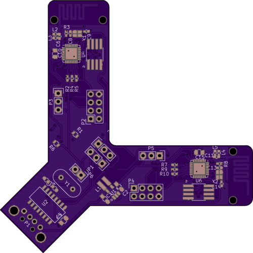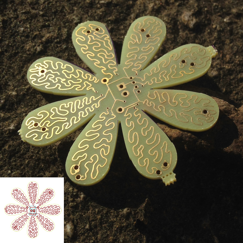
I designed the board above for my solar flower kit. It was partly an experiment is designing a weird shaped PCB, with funky traces and complex edges.
The process is kind of messy, and requires command line tools. If you’re a graphic designer and would like me to do this for you, click here. If you want to do this yourself, my notes are below.
The board edges have to be imported into Kicad separately from the graphics. You can only import DXF files. I use Inkscape to design the board edges and then export them as DXF. In Kicad in PCBnew select “File->Import->DXF” and import the DXF into the “Edges.cuts” layer.
First, I designed the flower shaped edge cut in Inkscape. In recent versions of KiCad it’s pretty easy to import the edgecuts. Firstly create your edges in Inkscape, ensure that the design is a simple line drawing and save it as a DXF file. Then just select “File->Import->DXF” in KiCad, and import the DXF into the Edge.cuts layer.
Creating interesting looking traces is more difficult. Kicad doesn’t really have a concept of non-straight line traces, and pads are similarly limited. There’s a tool in Kicad called “Bitmap2Component” which is ok for basic logos, but it doesn’t work that well with vector graphics.
For graphics I therefore use svg2mod. This is a neat little command line tool which takes a vector image into a Kicad component composed of a bunch of straight-line segments. After you’ve downloaded the tool you can run it as follows on an SVG:
./svg2mod.py -i ~/design.svg -o ~/design.mod -p 0.1
The “-p” parameter determines how many segments a curve is broken into, and may require some experimentation. svg2mod also works with multi-layer SVG files. You can create mask, copper, and silk layers and import them all into the Kicad component (the svg2mod readme specifies all the layer names you need to use).
You can them import the .mod component into Pcbnew and place it as you would any other part. In my case, I’d mark locations where LEDs should sit on the Inkscape design. I then placed LEDs over these in Pcbnew, this ensures that the drill holes get created correctly. I also had a small layout in the center of the board, the traces designed in Inkscape therefore needed to be manually aligned, and of course your DRC never passes.
That’s the basic process, and while it’s pretty messy but it works and you can create some entertainingly odd PCBs this way.