Archive for the ‘Uncategorized’ Category.

iNanoBio

Today I picked another company from my list of active DNA sequencing companies, iNanoBio!

INanobio is a Arizona State University (ASU) spinoff company. As far as I can tell from SEC filing [1] they’ve raised about 500KUSD. SEC filings also indicate they they were looking to raise 4MUSD in 2017, but I couldn’t see evidence that this has closed.

Technology

A significant challenge for nanopore sequencing is the speed at which DNA moves through the pore. One approach is to use enzymatic methods to slow the translocation of the DNA so it can more easily be read. iNanoBio is attempting to increase the read speed, so that they can sense DNA at 100Mhz to 1GHz as it passes through the pore.

As their patent [2] states, ionic mobility limits the rate you can measure changes in ionic current across a nanopore (they suggest ~10ms, which seems too slow, and don’t appear to provide a reference, if anyone has one I’d be most interested). They also suggest that tunnelling current measurement speed will be limited by quantum mechanical noise.

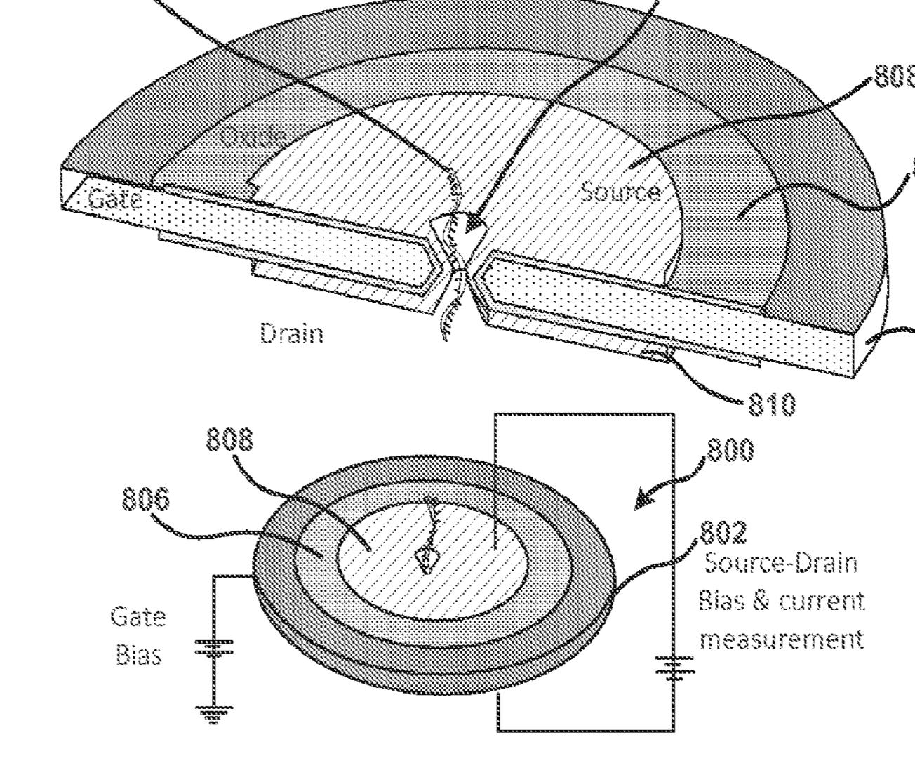
So instead of this they look at the base charges, specifically they say “dipole variations between individual bases”. The charges are detected by a novel FET transistor embedded in the nanopore. The nanopore has this sharp, conical shape. I assume this is designed to help avoid field contributions from multiple bases.

This sounds very neat, but I imagine generating the required signal level at >100MHz is challenging. It also feels like ensuring you only have charge contributions from a single (or small number) of basis would be problematic.

Never the less, if it works it’s a very neat idea. A 2014 youtube video suggests that they should be ready for research applications this or next year [3]… so I’ll keep an eye out!

Notes

[1] https://www.sec.gov/cgi-bin/browse-edgar?company=inanobio&owner=exclude&action=getcompany

[2] https://patents.google.com/patent/US20150060952A1

[3] https://www.youtube.com/watch?v=CwDdKhkQ-NE

QuantumDx

Building on from my list of sequencing companies in this post I look briefly at QuantumDX!

Business

QuantumDX Group was incorporated in March of 2008 [1]. In May 2009, they licensed nanowire FET IP, for use in DNA sequencing [2] from Nanosys. They also appear to have acquired a DNA testing service company (NorthGene limited).

November 2016, they received funding from Bill and Melinda gates foundation. Accounts state that they lost ~2.3MGBP in 2017, so their yearly burn rate seems to be about 3M GBP.

Their accounts state that they have operations in the UK, US and Singapore, and that commercialisation on a “research use only” basis is scheduled for 2018.

They raised 12MUSD [3] at the end of 2017. Given their previous burn, and cash in the accounts, my best guess would be that they’d have somewhere in the region of 10MUSD in the bank at present. Crunchbase lists them has having raise 26.3MUSD in total [4]. Investors include Barclays Global Investors and Helsinn Investment Fund SA.

QuantumDX also attempted to raise funds from Crowdfunding in 2014 [5], it appears at this point they had only raised from angel investors and grants.

Technology

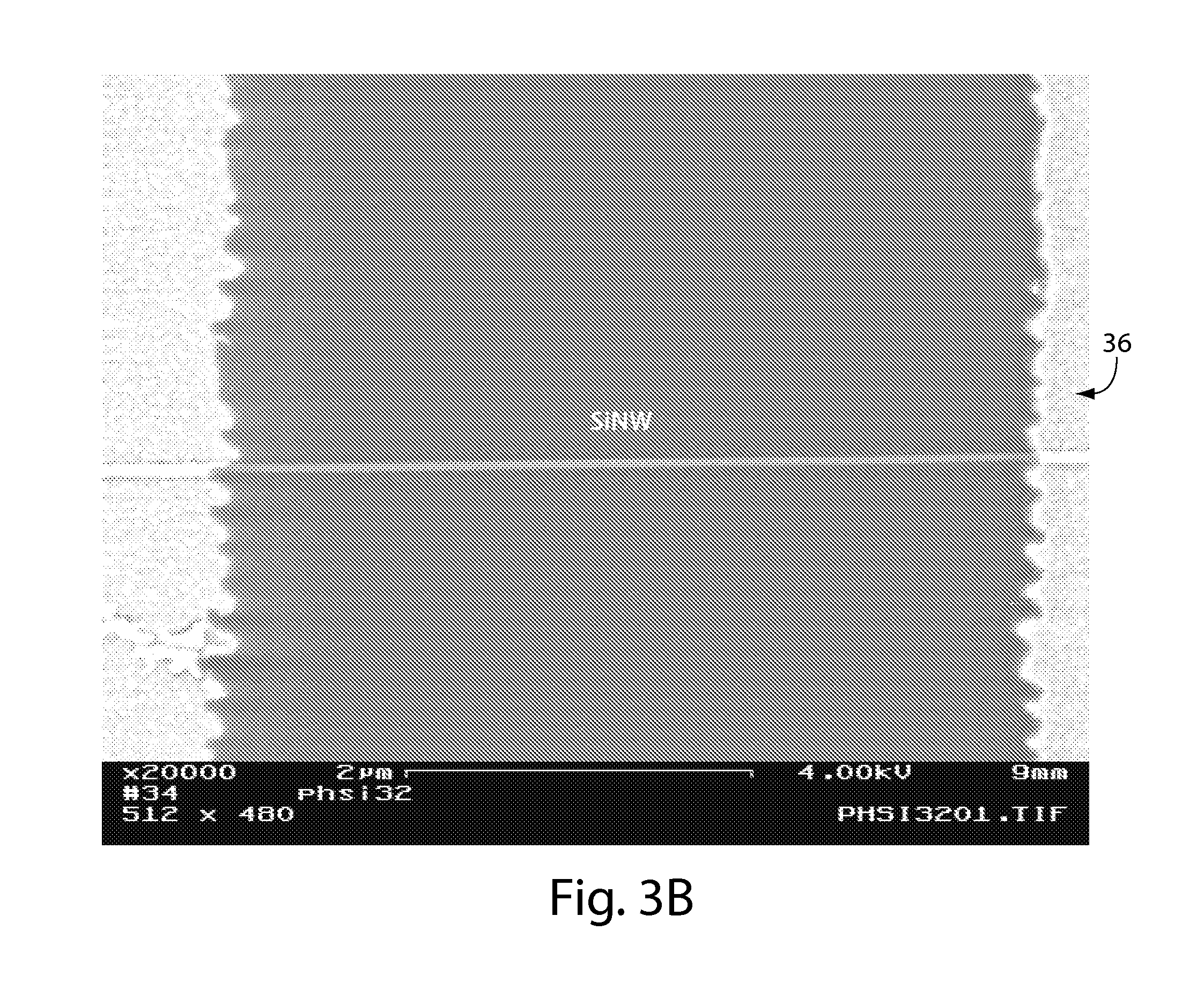
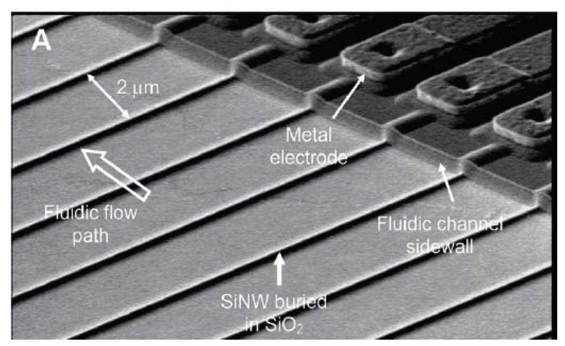
The QuantumDX technology appears to use FET nanowires for charge detection. The nanowire IP is licensed from Nanosys, while the QuantumDX patents don’t appear to show any SEM images of real structures, the Nanosys patents do [7] and are therefore a useful reference.

A number of structures are described in the patents, but the most relevant appear to be single nanowires stretched between electrodes (as I understand it, without doping and with no backing gate):

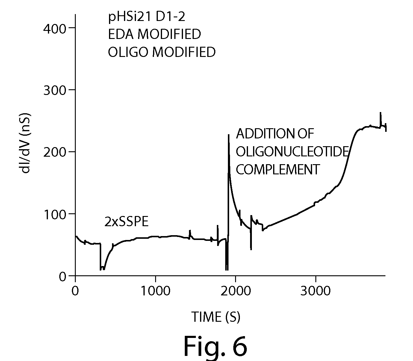
The patent also shows what appears to be real data of a nanowire complementary oligo hybridising to a probe on a nanowire:

From what I can tell, the presence of DNA (or any charged molecule) alters the resistivity of the nanowire. The nanowire contain very few charge carriers. This means that any nearby charges will have a significant effect on the flow or current through the nanowire. DNA being a charged molecule will effect the conductance of the nanowire, which is what you can see in the figure above.

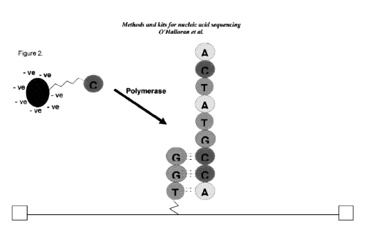
The QuantumDX patents describe a system that uses this effect to build a sequencing platform  (or potentially a probe based detection platform). The sequencing scheme appears to be standard sequencing-by-synthesis. Bases are added and incorporated into a template, and the increase in charge is detected. A number of patents refer to a “charge mass reporter moiety”. I guess detecting the single base charge may be problematic, so they can have a charged label attached to the bases to increase the amount of signal. I didn’t see anything that looked like real data in recent patents (but I’ve not looked very hard). A typical schematic of the system is shown below:

The system could obviously either be single molecule or work on clusters/amplified DNA. If the system could be made to work with single molecules (and ideally unlabelled nucleotides) I can see that it could be quite interesting, perhaps allowing quite long reads to be generated.

It’s an interesting approach, and I look forward to seeing more data as it appears.

Update: this presentation and some nice figures, including the following SEM image:

Notes

[1] Companies House: https://beta.companieshouse.gov.uk/company/06523152 and https://beta.companieshouse.gov.uk/company/07067899

[2] “QuantuMDx Group (QMDx) today announced that QMDx has signed a non-exclusive license agreement with Nanosys for several patents and patent applications related to the use of nanowires for biosensors.

The core intellectual property involves the use of nanowire-based field effect transistors (FETs) as biosensors, which were derived from the work of Dr. Charles Lieber, a professor of chemistry at Harvard, a pioneer in nanotechnology, and one of the founders of Nanosys.

Under terms of the agreement, QMDx has secured worldwide rights for the use of nanowires for DNA sequencing and detecting biomarkers associated with disease. In exchange, Nanosys has received an upfront license fee and downstream royalty payments. No other financial details of the deal were disclosed.”

https://www.biospace.com/article/releases/nanosys-inc-licenses-nanowire-technology-to-quantumdx-group-for-next-generation-diagnostic-and-sequencing-technologies-/

[3] https://quantumdx.com/news/quantumdx-raises-12m-and-strengthens-board-as-company-eyes-commercialisation-of-q-poc-portable-mdx-platform

[4] https://www.crunchbase.com/organization/quantumdx-group#section-overview

[5] http://www.bio-itworld.com/2014/2/12/quantumdx-launches-moldx-indiegogo-campaign.html

[6] “The potential of nanowires was demonstrated in a 2001 Science paper authored by Harvard University’s Charles Lieber and colleagues. That proof of principle, according to Burn, showed that changes of impedance in silicon nanowires could record the arrival of a biomolecule. Recently, QMDx announced the exclusive license of intellectual property from Lieber’s company, Nanosys, of the diagnostic and sequencing applications of nanowires and nanotubes. (The arrangement succeeds a non-exclusive IP deal previously announced in 2009.)”

http://www.bio-itworld.com/issues/2012/jan/a-quantumdx-leap-for-handheld-dna-sequencing.html

[7] https://patents.google.com/patent/US20110315962A1

“FIG. 6 shows the conductance for a silico nanowire having a surface modified with an oligonucleotide agent reaction entity. The conductance changes dramatically where the complementary oligonucleotide analyte binds to the attached oligonucleotide agent.”

DDC112 Board Design/Bring Up

The DDC112 is a integrating current input ADC. You can use it for acquiring small currents (of the range of femto to picoamps (or larger if you want). Often a trans-impedance amplifier (current to voltage converter) would be used for this purpose. However the DDC112 doesn’t work like this…

The DDC112 collects current on a capacitor. It then periodically switches the capacitor over to a ADC, and starts collecting charge on a second capacitor while acquisition takes place. So, rather than having “gain” the switched current integrator has two parameters you can vary. The size of the capacitor and the time you integrate over.

The DDC112 has a number of build in capacitors, and you can also add your own externally. The DDC112 is really designed for photodiode applications. The series contains parts with 100s of channels, and built in ADCs. You’d use these for photodiode array systems, things like X-ray machines, CT Scanners etc.

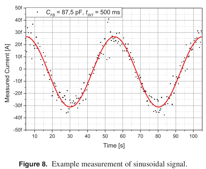
However, I’m more interested in alternative applications. Things like scanning tunneling microscopes, or nanopore systems. Both these applications require the acquisition of picoamp current traces at a few kilohertz. Googling around, I found an interesting paper where they evaluated the DDC112 for use in an STM. They show a 50 femtoamp sine wave (sampled at 2Hz) which I thought was pretty cool:

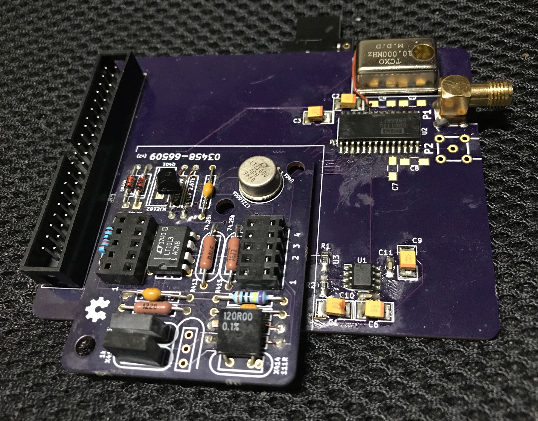
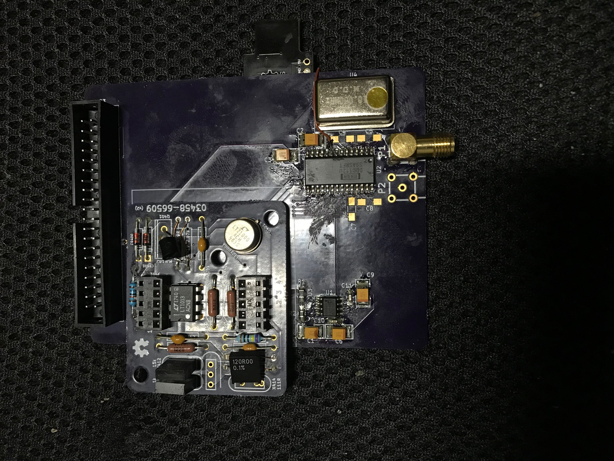
Various other sources indicated that you should be able to get about 2 picoamps of noise at 1KSPS. Unfortunately I’ve not seen any board designs or code generally available. So I’ve started putting my own design together and doing some basic testing. Here’s the completed board:

Everything is probably overkill here… The DDC112 requires a 10MHz clock, so I used a 10MHz TXCO… totally unnecessary. But I was curious to play with a TXCO. I may well end up swapping it out later.

The DDC112 has continuous and non-continuous modes of operation. I wanted to run in continuous mode, constantly taking samples. To do this, you need to toggle the CONV pin, at a fixed frequency. This controls the switching (switching between collecting charge on one capacitor or another).

This frequency should be somewhat synchronized with the main clock. If I was using a fast (>100MHz) processor, I could probably just synthesize the 10MHz clock and the CONV trace. But i wanted to retain flexibility (and have currently been driving the board with an Arduino Mega). For this reason I decided to add a clock divider/generator.

For this I used an ATTINY85. I modified a digispark to use the same oscillator as the DDC112 as documented here. Currently I’m using it to generate a 1Khz CONV signal.

With these two signals in place, the DDC12 will acquire data, and pull DVALID low when an acquisition is ready. You can use DVALID to trigger and interrupt, and transfer the data to a microprocessor over SPI.

I’ve included board designs, and a dump of the code I used for testing in the notes below. A number of hacks were required on the board (re-routing DVALID to an interrupt capable pin, adding the digipark frequency generator). But they’re here for reference.

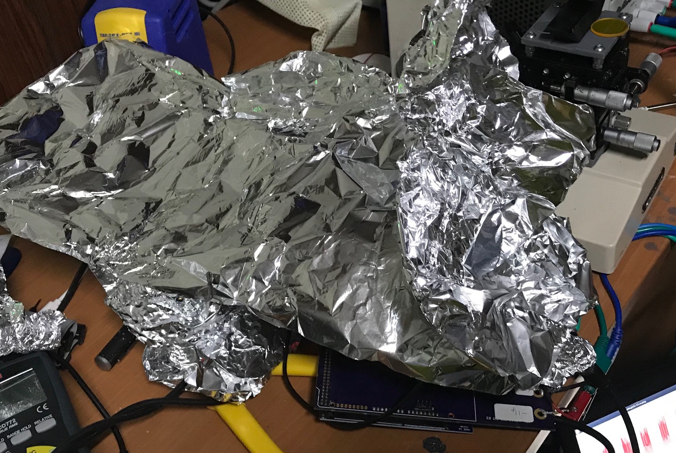
I’ve completed some very basic tests. The board seem capable of acquiring picoamp level signals. My shielding isn’t great:

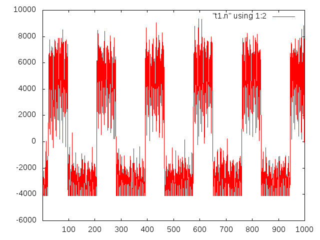
But the first traces don’t look too bad, here’s a 5Hz 1nA square wave, sampled at ~1.2KSPS:

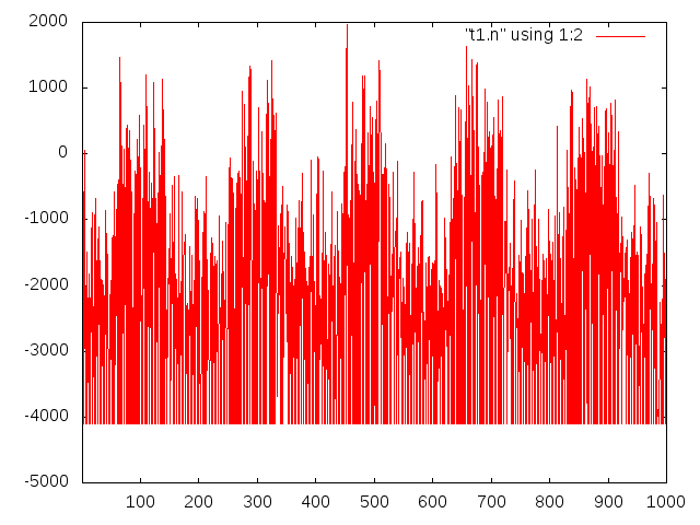
And here’s a 200pA square wave at the same:

The 200pA trace isn’t as clean as I’d like it to be, but I think if I clean up my test setup I should be able to improve things. In particular, I’m using a 100MOhm resistor to generate in input current. Likely using a larger resistor (and larger/cleaner voltage over it) would help a little. Obviously the shielding and board layout also needs work.

If you have a potential application for this board, please contact me. It would be interesting to collaborate.

Notes

Board designs (unchecked): DDC112_boards.tar

Arduino Mega code:

#include 
#include   

void setup() {  

  // put your setup code here, to run once:
  Serial.begin(115200);
  SPI.begin();
  SPI.beginTransaction(SPISettings(10000000, MSBFIRST, SPI_MODE0));

  // range pins
  pinMode(A7,OUTPUT);
  pinMode(A6,OUTPUT);
  pinMode(A5,OUTPUT);

  // range setting
  digitalWrite(A7,HIGH);
  digitalWrite(A6,LOW);
  digitalWrite(A5,LOW);

  pinMode(2,OUTPUT); //TEST
  pinMode(13,INPUT);//CLK
  pinMode(4,OUTPUT); //DXMIT
  digitalWrite(4,HIGH);
  pinMode(5,INPUT);  //DVALID, old routing

  digitalWrite(2,LOW); //TEST PIN LOW=off

  attachInterrupt(1, read_data, FALLING); //DVALID (re-routed)
}

long int a=99;
long int b=99;
long int c=99;
long int d=99;
long int e=99;

bool read_ok=false;
long int in1 = 0;
long int in2 = 0; 
void read_data() {

  // READ DATA
  digitalWrite(4,LOW);  //DXMIT

  a=0;
  b=0;
  c=0;
  d=0;
  e=0;
  a = SPI.transfer(0);
  b = SPI.transfer(0);
  c = SPI.transfer(0);
  d = SPI.transfer(0);
  e = SPI.transfer(0);

  digitalWrite(4,HIGH);
  in2 = (a << 12) | (b << 4) | (c >> 4);
  in1 = ((c & 0x0F) << 16) | (d << 8) | e; 

  in1 -= (1 << 12);
  in2 -= (1 << 12);
  
  
  read_ok=true;
}

void loop() {

  //1 DCLK_INF       SCLK
  //2 DVALID_INF     3 (patch)
  //3 SDIN           SDIN
  //4 DXMIT_INF      4
  //5 DOUT_INF       SDO
  //6 CONV_INF       3 
  //7 NC             
  //8 TEST_INF       2
  //9 NC
  //10 RANGE0_INF    AD7
  //11 NC
  //12 RANGE1_INF    AD6
  //13 NC
  //14 RANGE2_INF    AD5

  if(read_ok) {
    Serial.print(in2);
    Serial.print(" ");
    Serial.println(in1);

    read_ok=false;
  }
}

ATTINY85 code:

void setup() {
  // put your setup code here, to run once:
  pinMode(PB0,OUTPUT);
}

void loop() {
  // put your main code here, to run repeatedly:
  for(;;) {
    digitalWrite(PB0,1);
    delayMicroseconds(500);
    digitalWrite(PB0,0);
    delayMicroseconds(500);
  }
}

Reprogramming a ATTINY85 to use an external oscillator using the Arduino IDE

I’d read about using PIC series microprocessors as clock dividers. For a project I’ve been working on I wanted to do the same thing. I find working with PICs pretty painful so I thought I’d use the Attiny85 from a digispark I have.

The process is pretty straightforward, but I wanted to document it here.

In order to reprogram the ATTINY85 to use a different oscillator, you need an AVR programmer. It’s not possible to set the fuses using the digispark bootloader. An Arduino Uno (or a knockoff) can be programmed to be used as a device programmer for other AVRs. The Arduino ISP includes the software to do this under Examples->ArduinoISP.

You can then put a simple header together to attach to the ATTINY85. I recommend picking up a cheap SOIC8 clip from eBay. The wiring required is described here [1].

Here’s my version of this header:

With the ArduinoISP flashed onto your Uno, it’s now possible to reprogram the ATTINY85. The standard Arduino IDE does not include the board support package to do this however. You need to add the following under Preferences->Additional Board Manager URLs:

https://raw.githubusercontent.com/damellis/attiny/ide-1.6.x-boards-manager/package_damellis_attiny_index.json

With this installed you should be able to select the attiny under Tools->Boards. Also select Arduino as ISP as the programmer. You may need to reflash the bootloader to set the fuses (not sure if this is required or not).

In my case, I also wanted to use an External Oscillator (not external crystal) with the ATTINY85. The damellis package does not include support for this so I had to add it to boards.txt. The location of this file may differ on your system. On my Linux PC it was at:

~/.arduino15/packages/attiny/hardware/avr/1.0.2/boards.txt

I was using a 10MHz external oscillator, so I added the following:

ATtinyX5.menu.clock.external20=External Osc 10MHz
ATtinyX5.menu.clock.external20.bootloader.low_fuses=0xf0
ATtinyX5.menu.clock.external20.bootloader.high_fuses=0xdf
ATtinyX5.menu.clock.external20.bootloader.extended_fuses=0xff
ATtinyX5.menu.clock.external20.build.f_cpu=10000000L

I also need to wire up the oscillator of course. You can connect it to pin P3 on the digispark header. Of course, the oscillator and digispark will also need power. Here’s my board, all hacked up, and ready to go:

Notes

[1] Backup of wiring image from: here.