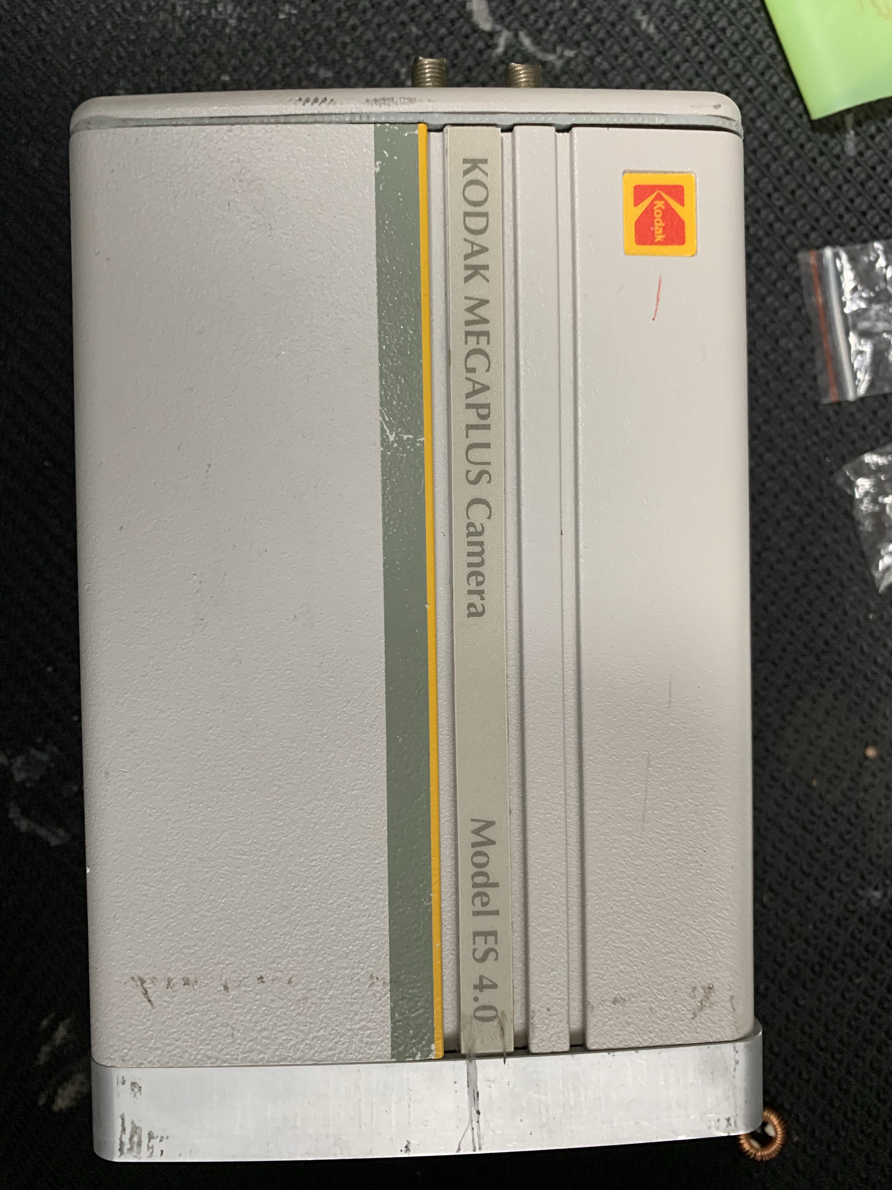
Kodak ES 4.0 teardown pics
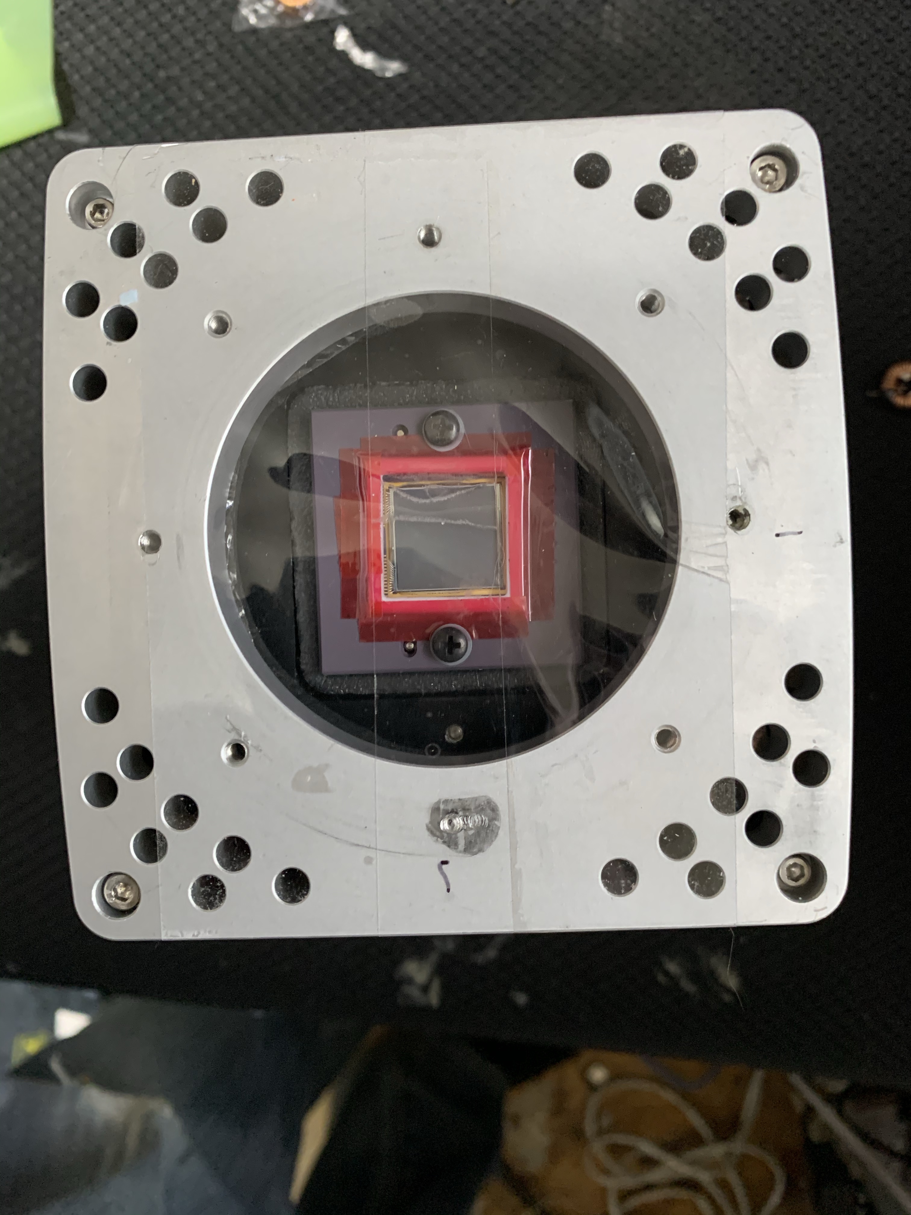
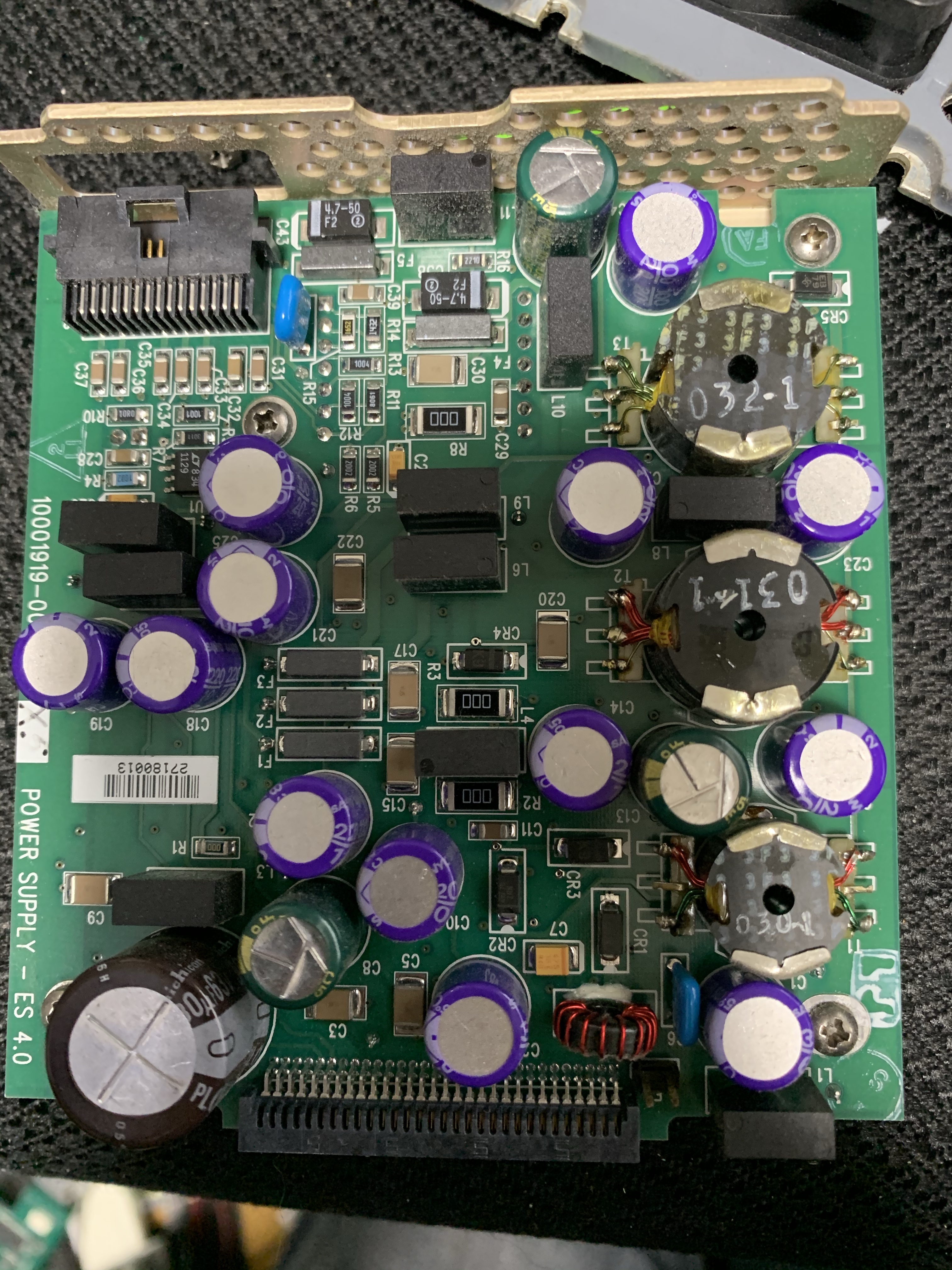
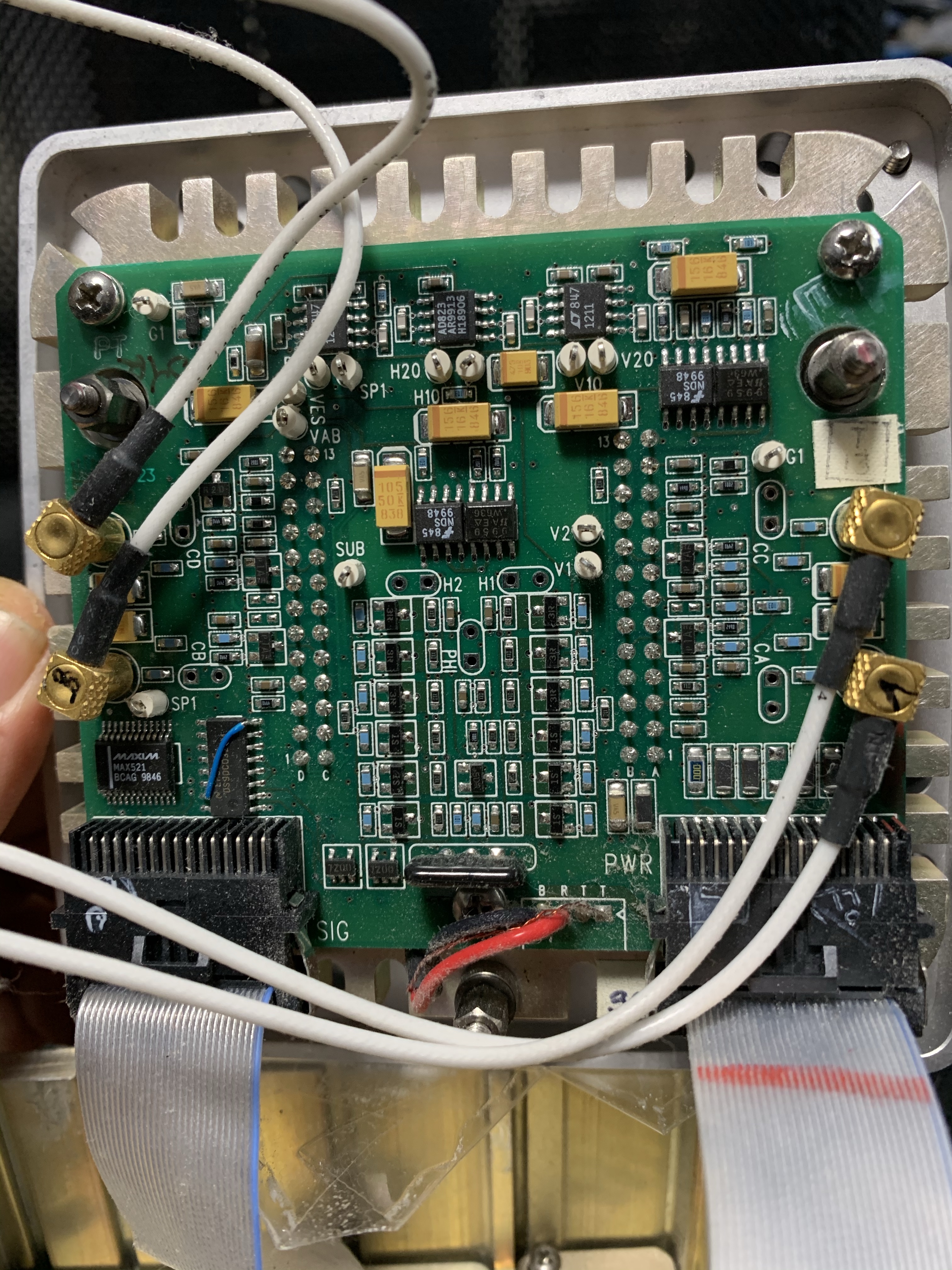
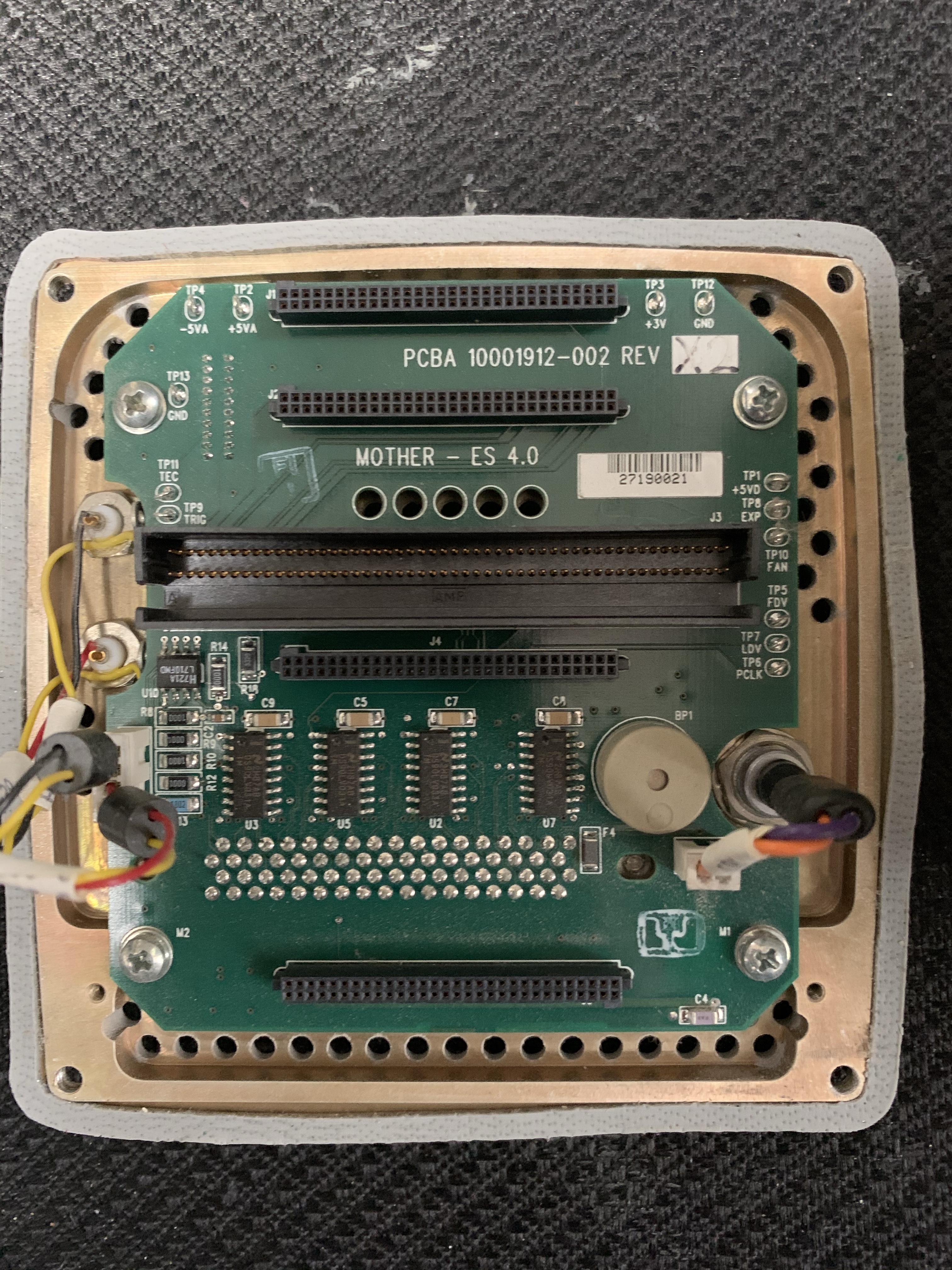
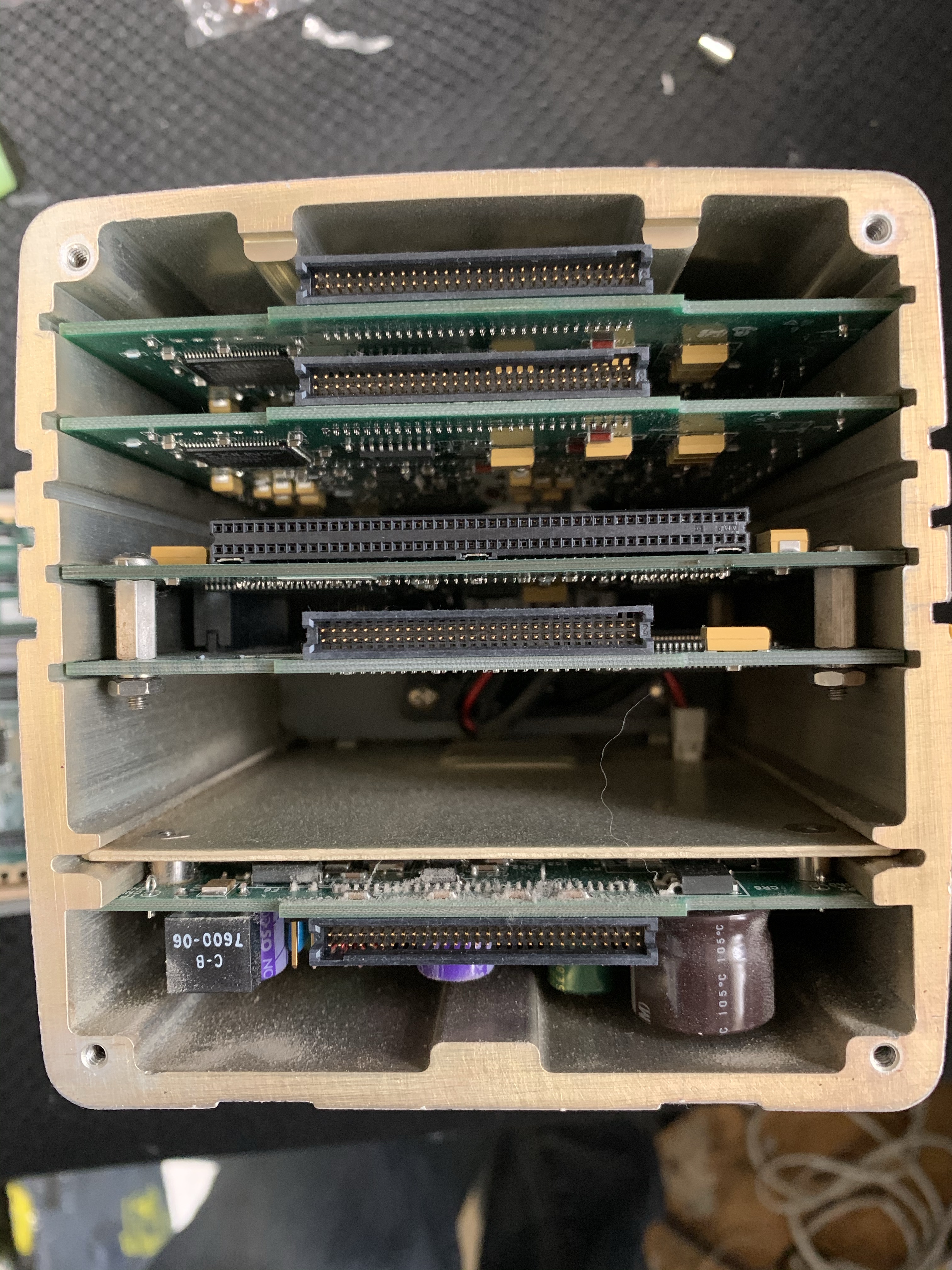
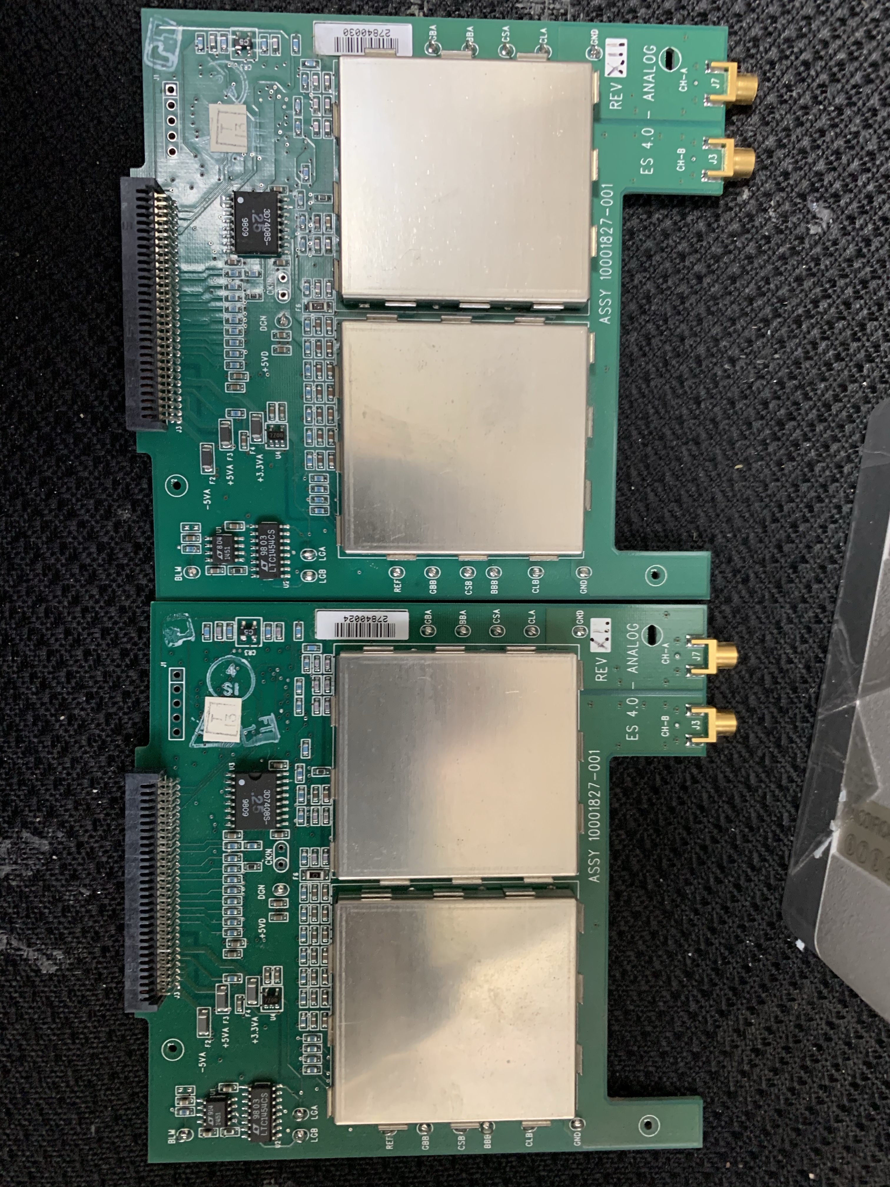
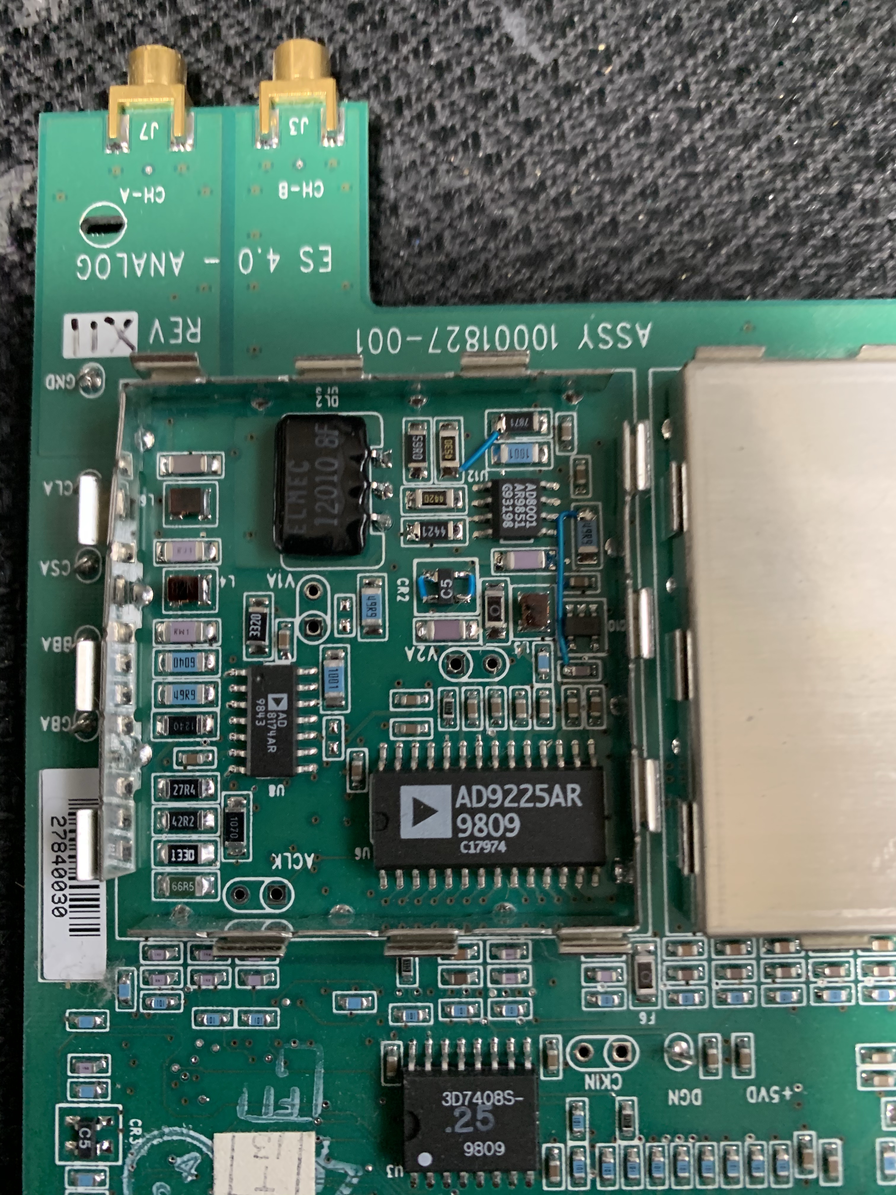
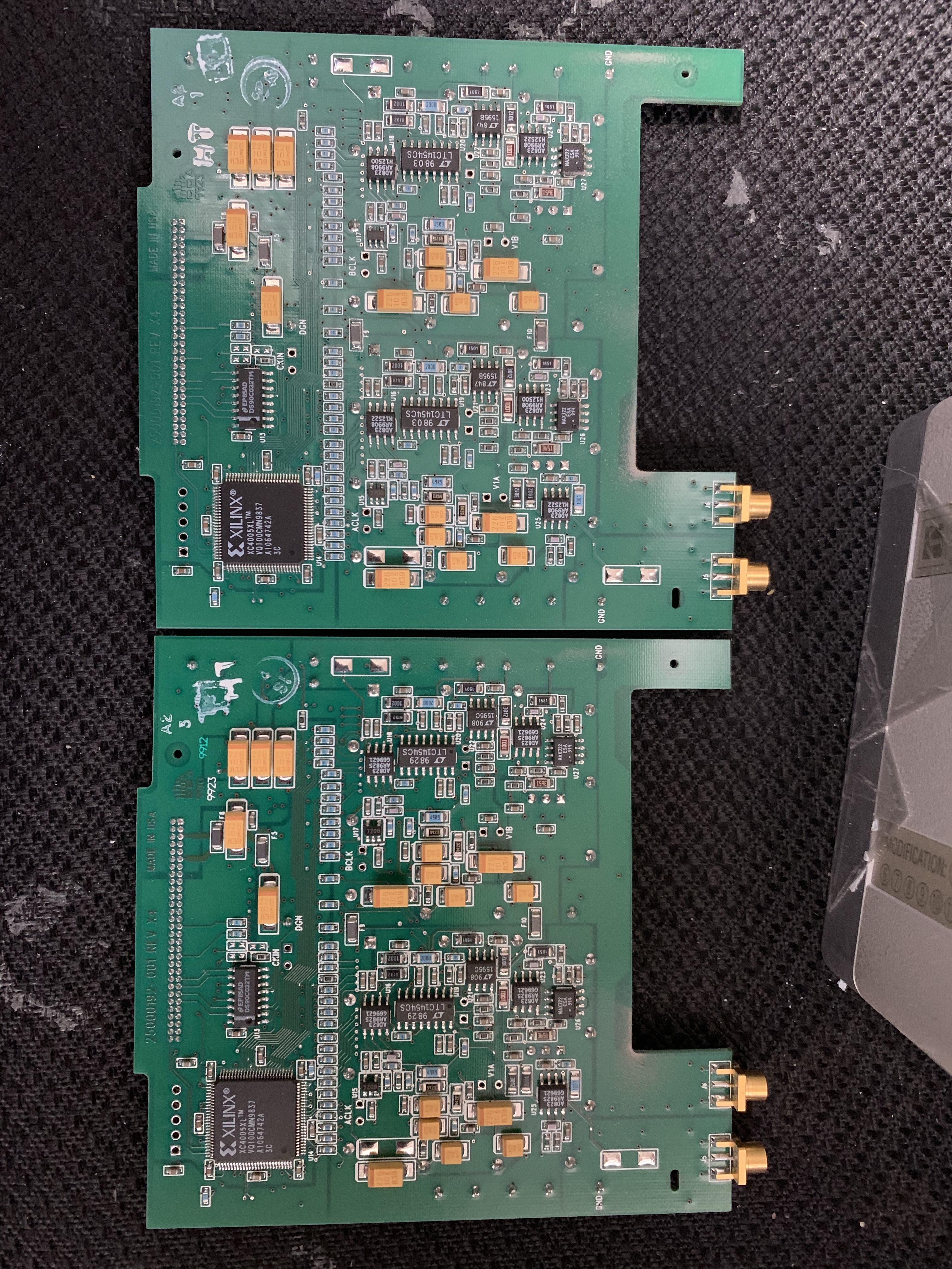
This post contains tear-down reference images for a Kodak Es 4.0 camera. From memory, the camera uses a KAI4000 image sensor. This is a 90s/00s era image sensor. The sensor effectively operates as 4 independent image sensors. For the fastest/most consistent readout you probably want to acquire images from all 4 quadrants at the same time. As such this camera duplicates analog and acquisition circuits four times. A AD9225 ADC is used, and four of these are present under shields.
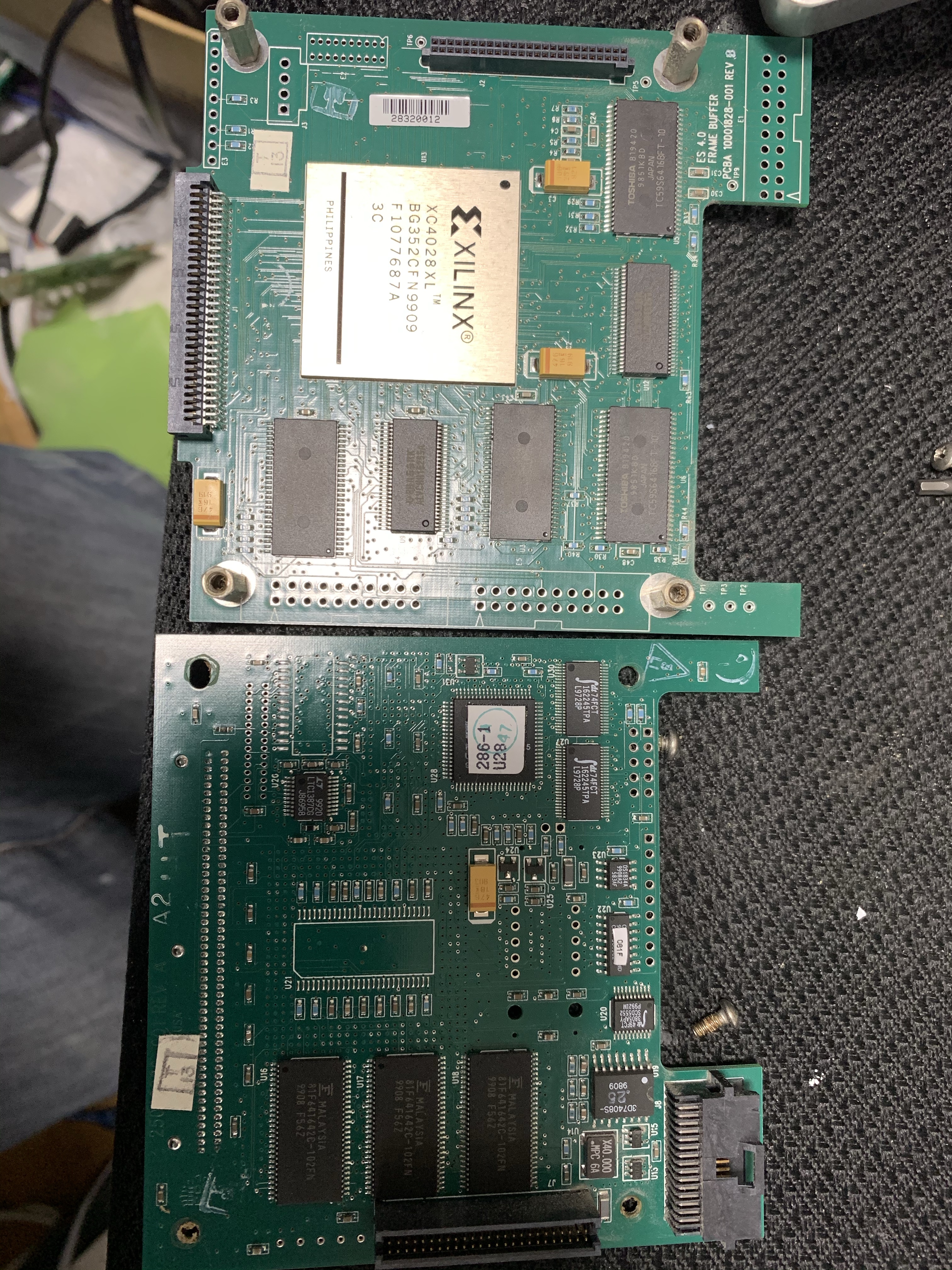
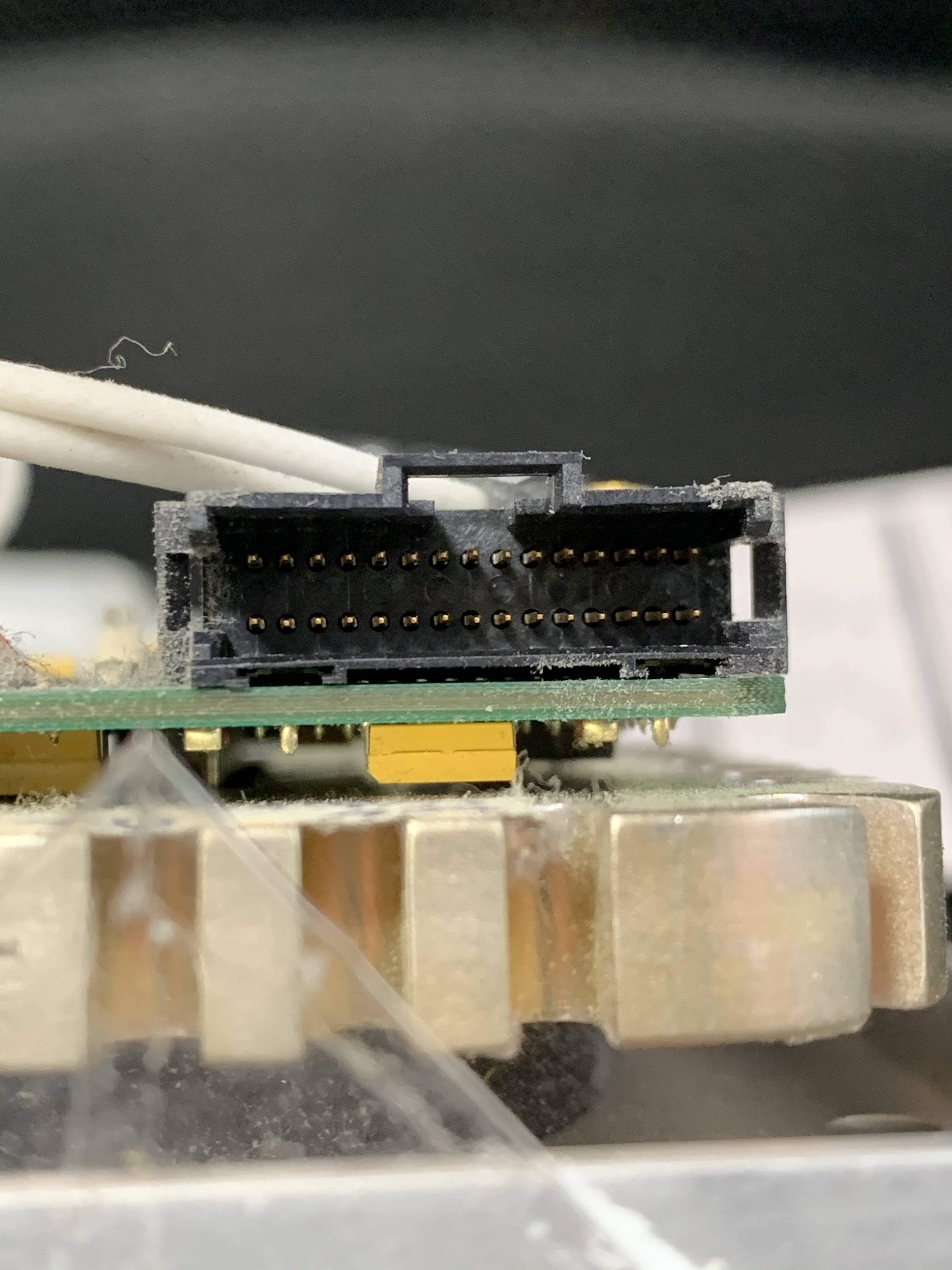
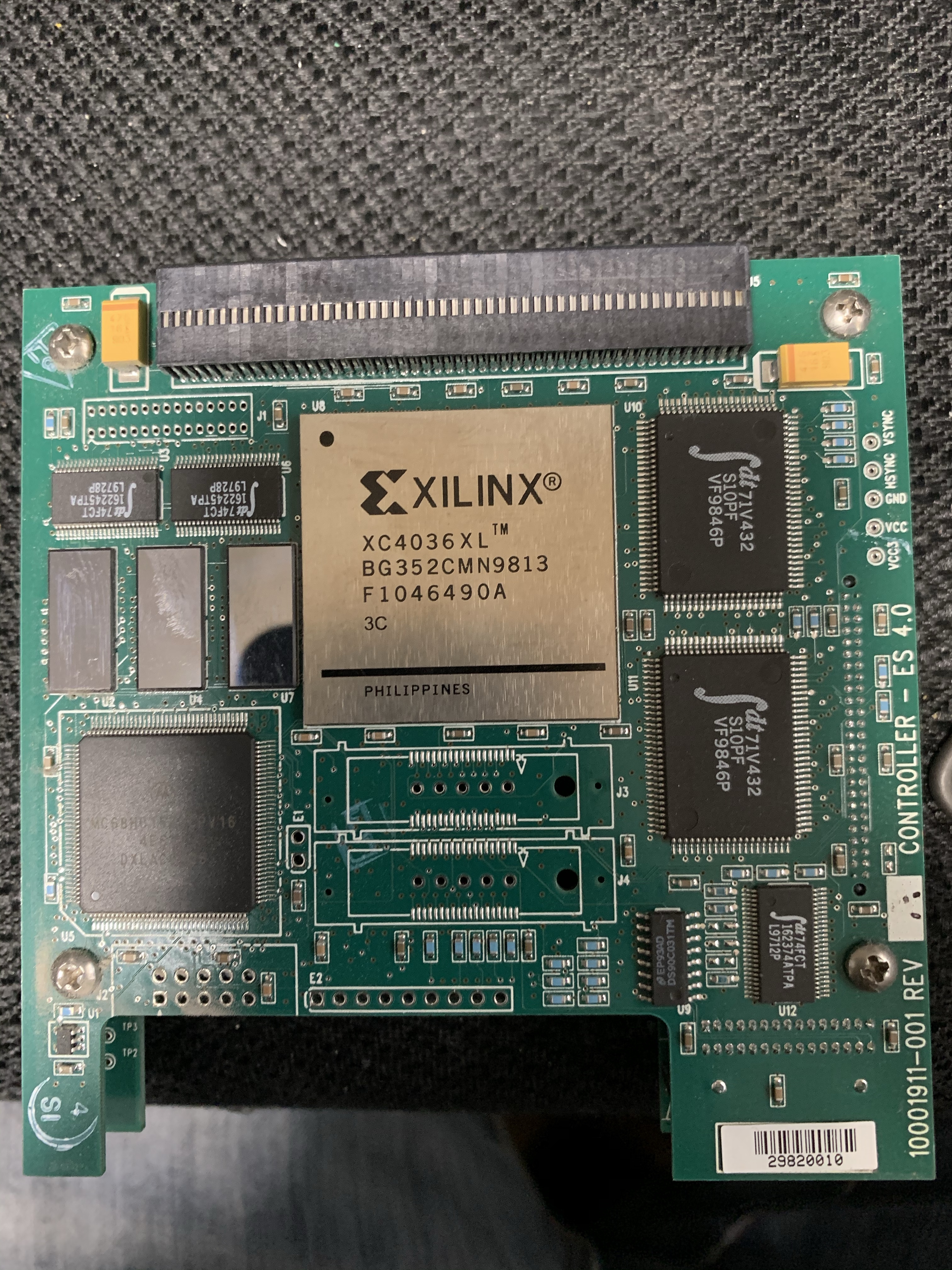
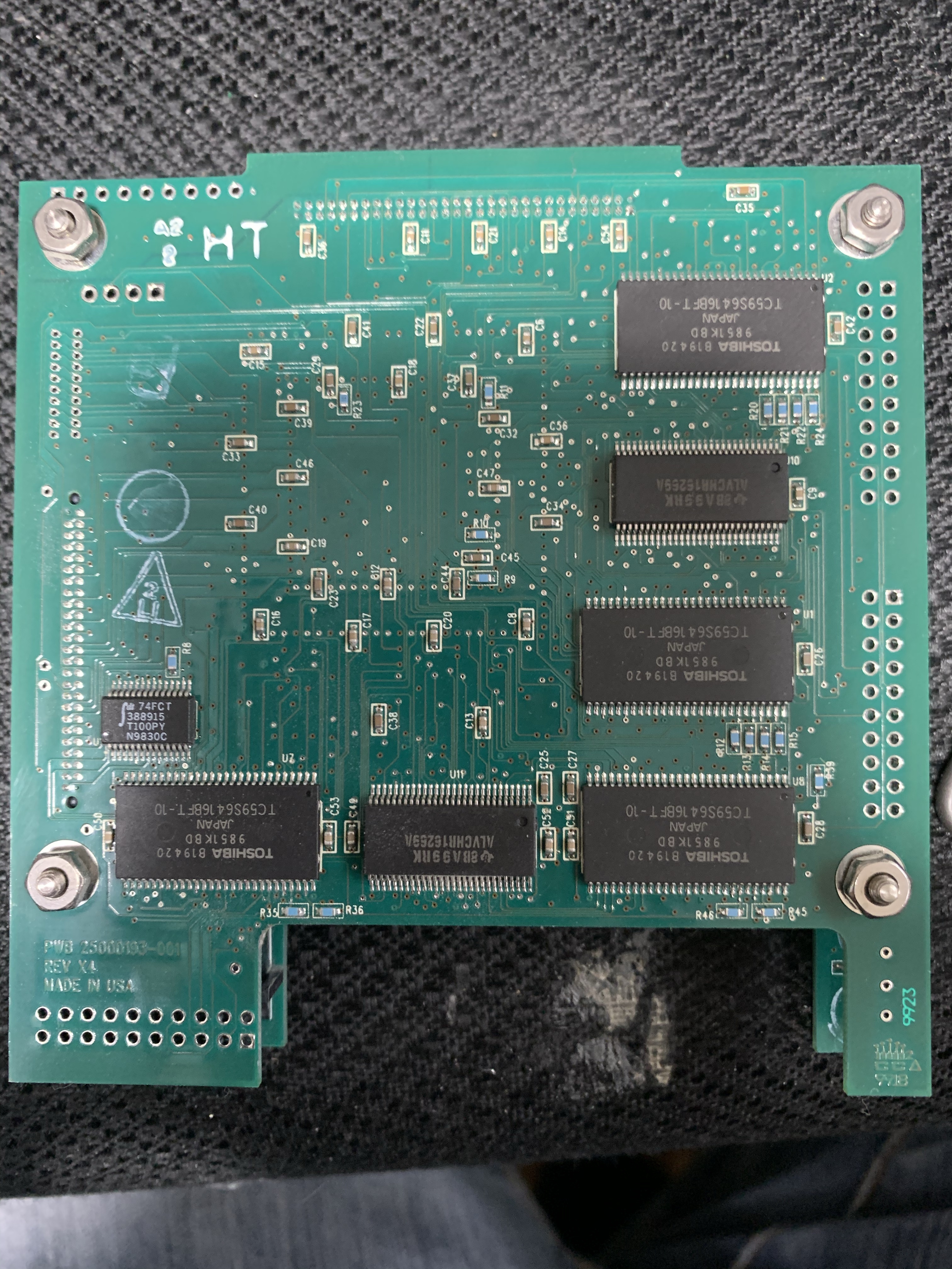
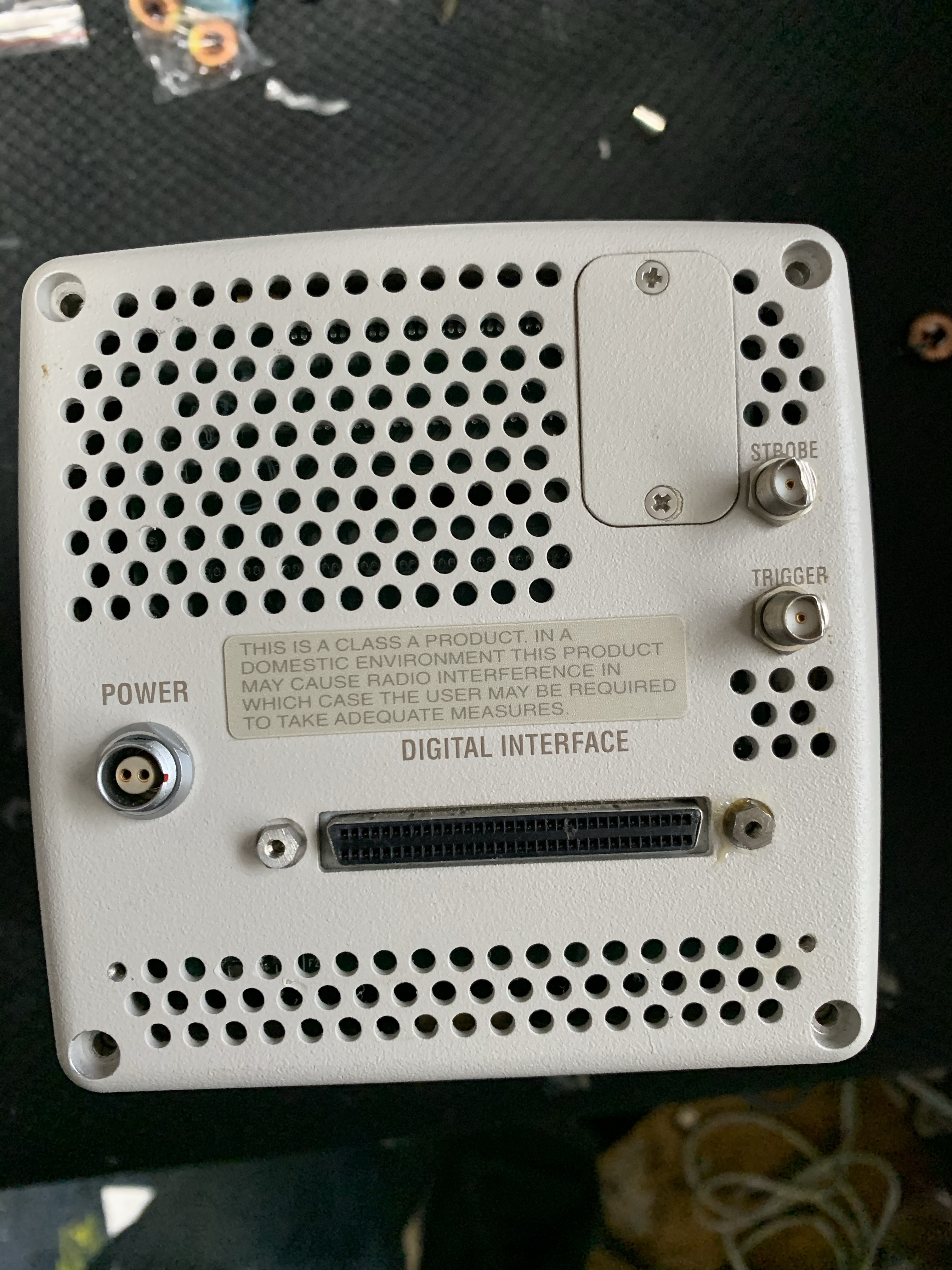
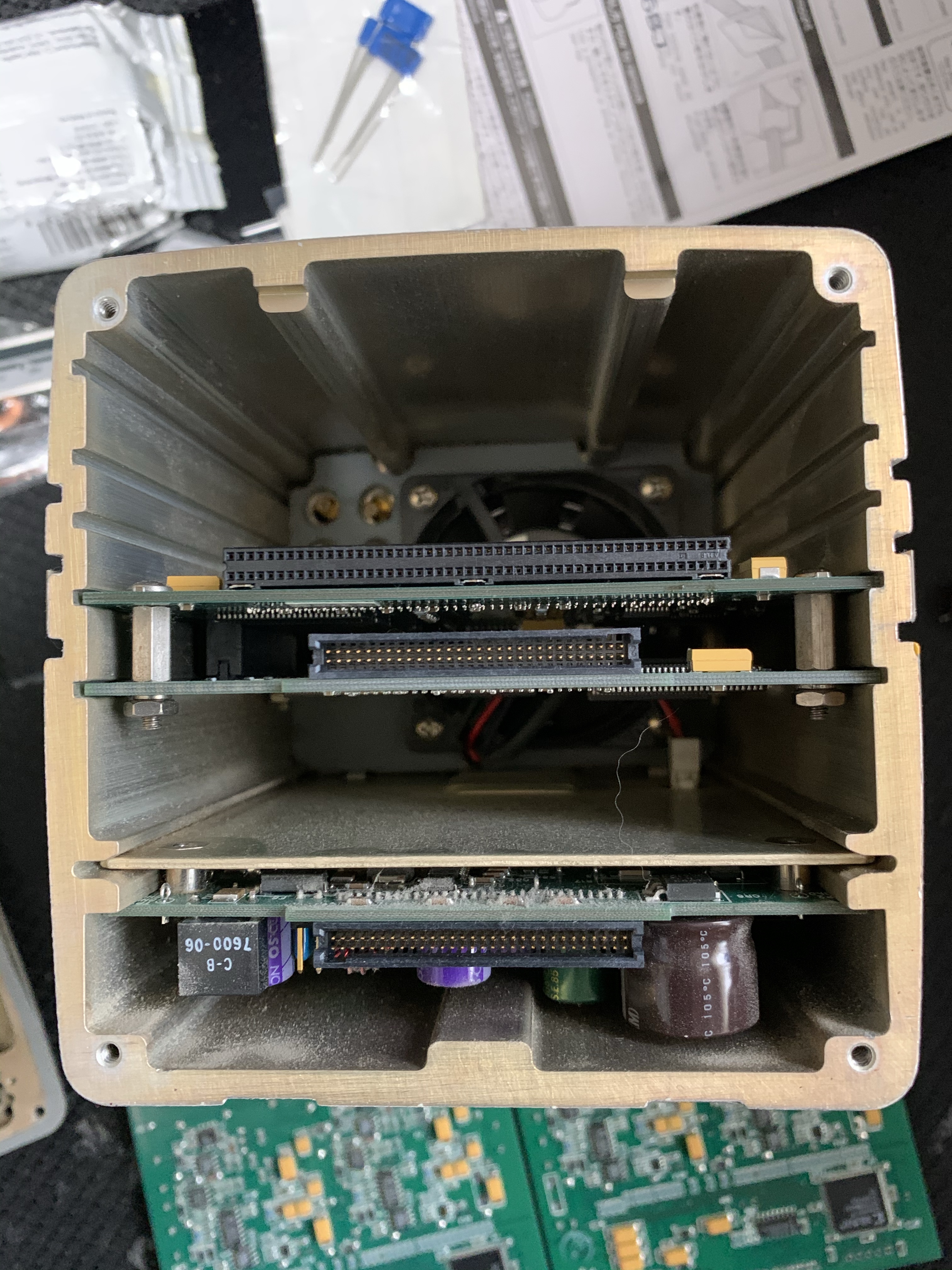
A bunch of Xilinx FPGAs are used to acquire data from the ADCs/send it to a host computer. I do not have the interface card required to operate this camera, so can’t test this.
The CCD is cooled using a TEC. Again from memory, the feedback does not appear to be an RTD. If I remember correctly a thermistor was embedded in the TEC block.
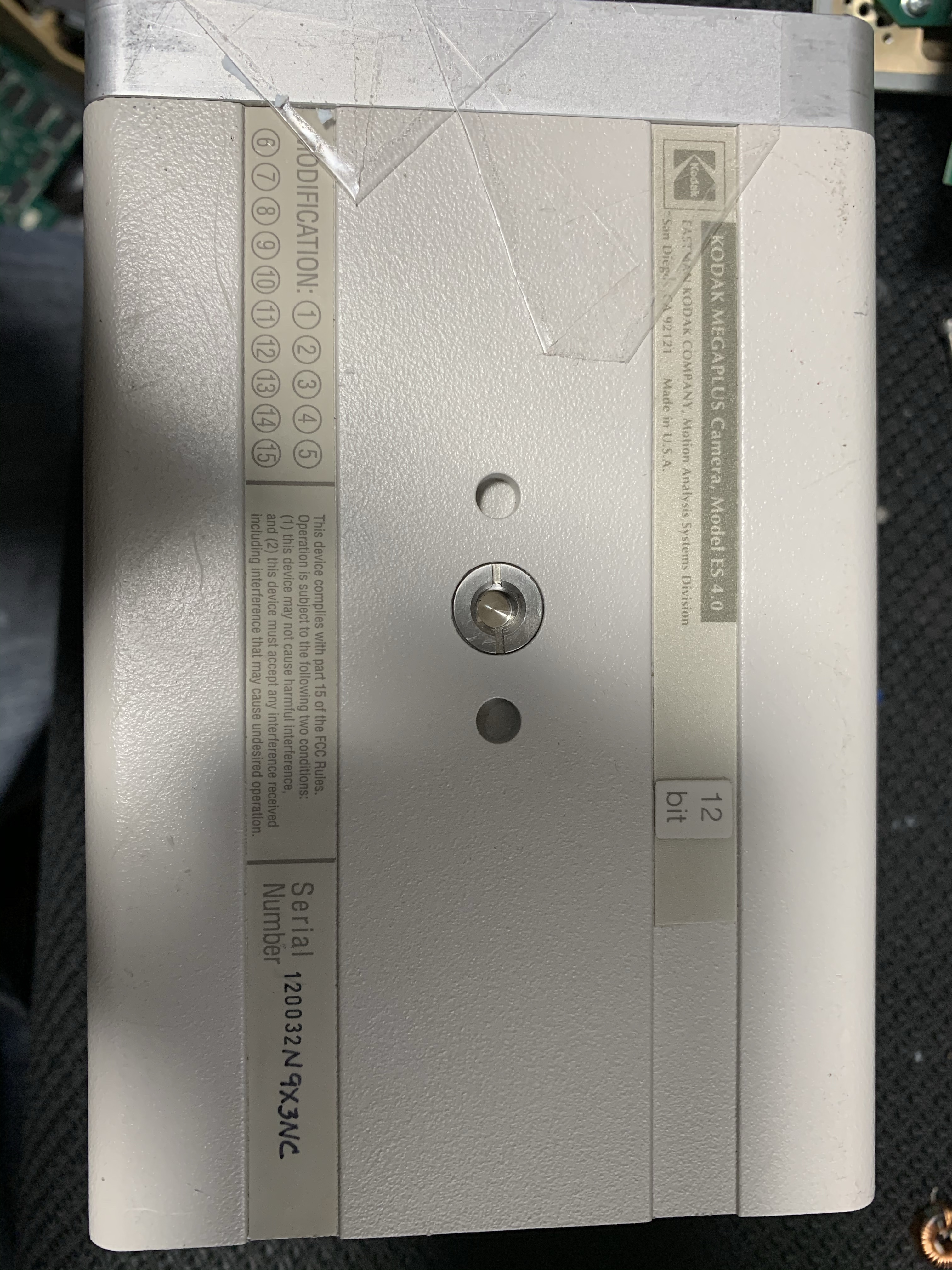
While this camera is branded by Kodak, I think I’ve seen similar units from Princeton/Roper. Possibly these were re-branded. However it seems like there may have been a number of acquisitions in the 2000s and perhaps someone acquired Kodak’s (scientific/industrial) camera unit…