Throwing the BME280 Combined Pressure/Humidity Sensor in a SEM
 Yesterday I decided to throw a BME280 in a SEM. We purchased the hackerfarm SEM a while back, but recently I’ve been getting a bit more use out of it.
I’ve also recently been getting interested in the BME280 combined pressure/temperature humidity sensor, and plan to make a board for my espusb design based around it. This seems to be one of the few MEMS humidity sensors on the market, and seems to perform very well.
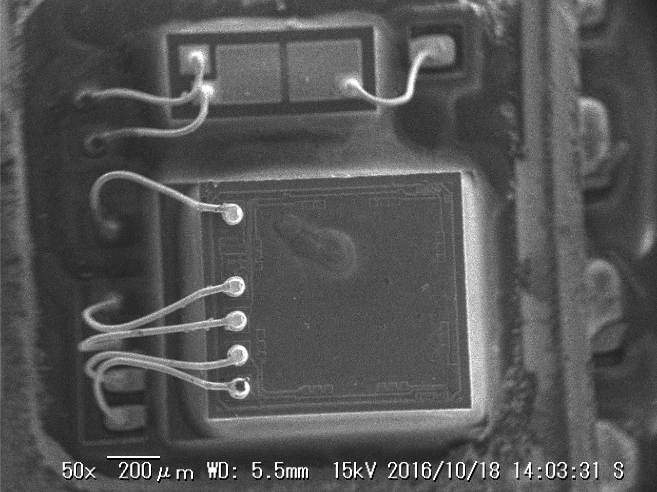
However it’s unclear exactly how the humidity sensing functions. So in the SEM it goes! The tiny can seems to contain 3 discrete dies. In the image to the right you can see the large lower die, and a much smaller upper die. Under the lower die it looks like there’s another die, I assume that’s the ADC/SPI/I2C interface controller. I’d guess that the sensors require some novel process, and are therefore fabricated separately.
 So… my gut feeling is that the lower die is a pressure sensor. Most MEMS pressure sensors appear to be based on a diaphragm with a piezo coating. I didn’t have time yesterday but I might try and investigate this die further in the future.
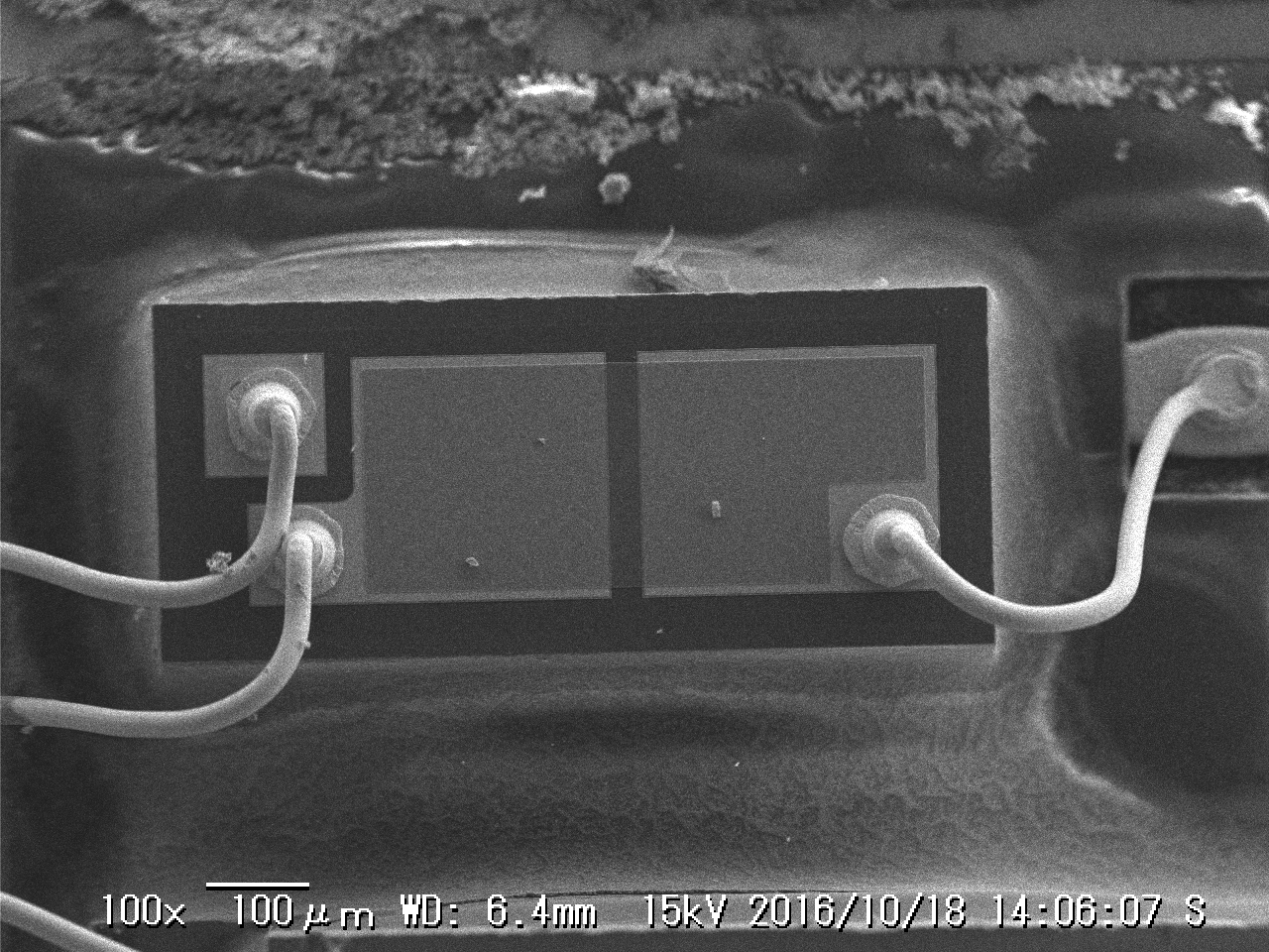
So I focused on the upper die, shown to the left, and found the construction to be surprisingly interesting.
It looks like there are 2 large pads with some kind of (I assume thin-film) placed over them.
This film was really interesting.
Moving up to 300x we can start to see structure in this film: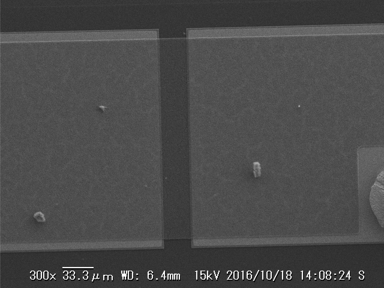
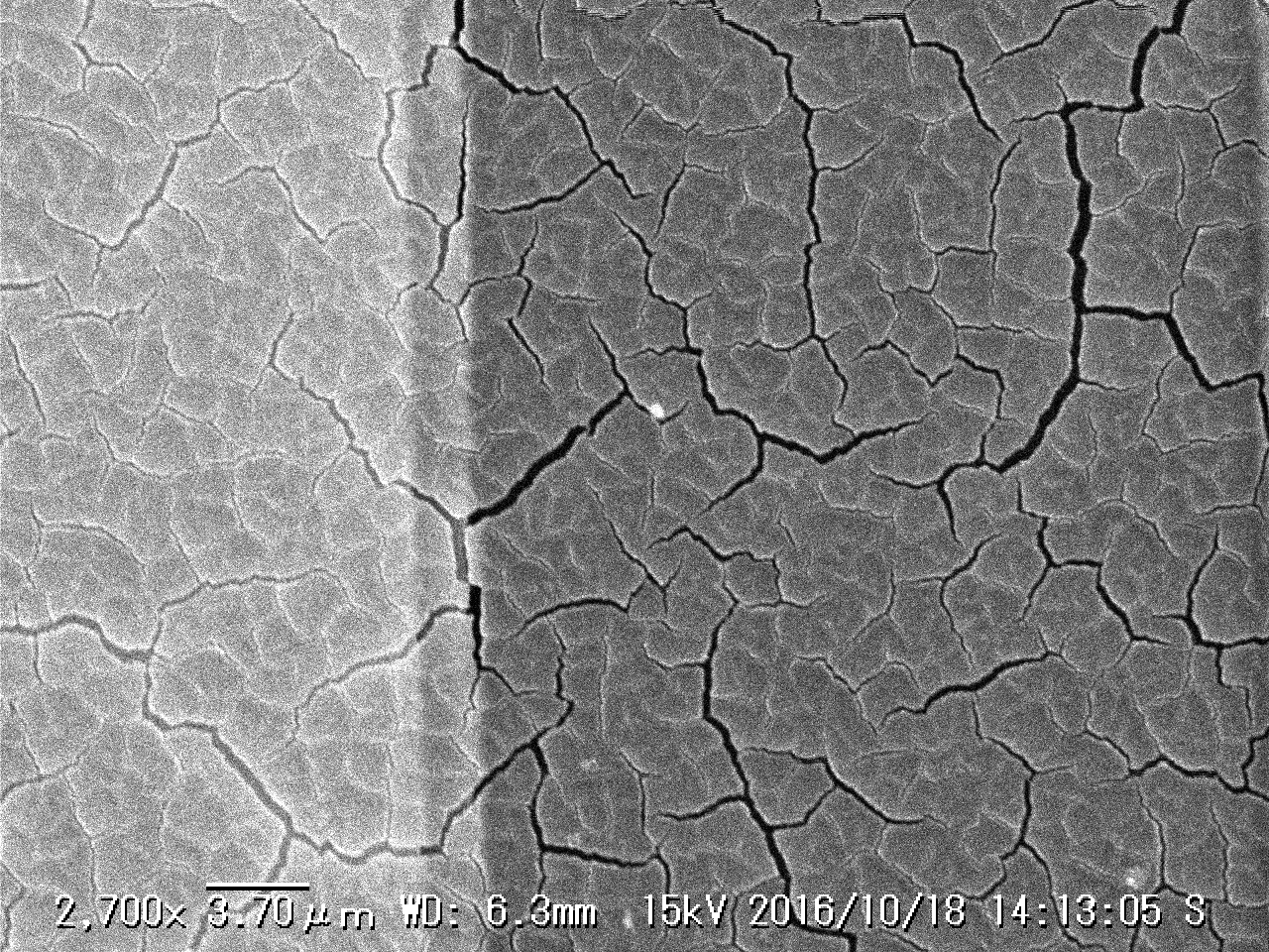
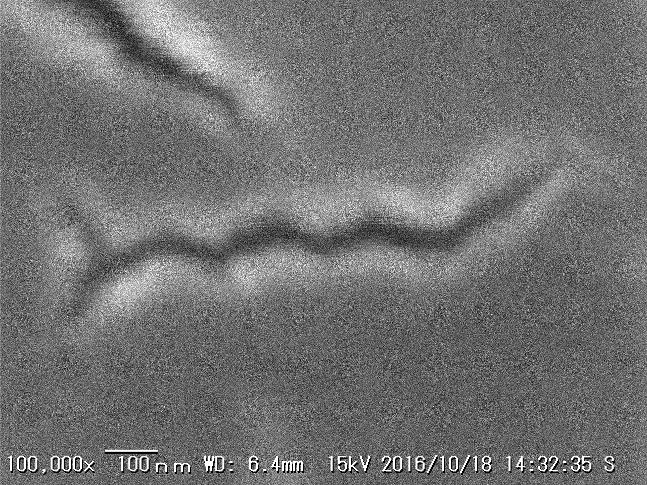
Zooming in further and approaching the diffraction limit we can see this really interesting almost fractal like, structure.
These cracks are really interesting, and I assume not just a manufacturing defect but a functional part of the surface. I’d kind of guess that these small pores allow water to be absorbed into the surface and change the resistivity or capacitance of the layer.
The fractures range from ~1 micron to <100nm wide. The image below shows a fracture at x100000.
I was curious to find out a bit more, while nothing is easily available online a patent search yielded some useful information. This patent from Bosch shows a very similar layout to the BME280:
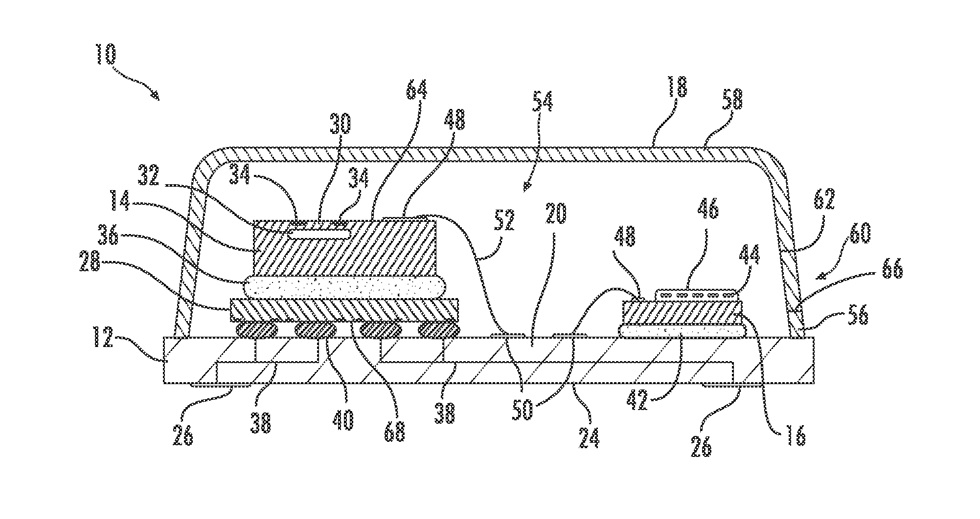
While that patent doesn’t cover the humidity measurement in detail it does contain the following paragraph:
“Humidity sensors are widely used in various fields to measure the amount of water vapor present in the air of a particular environment. Humidity sensors typically include a pair of electrodes separated by a dielectric material. The dielectric layer is formed of a material, such as polymer that is configured to absorb and retain water molecules at concentrations that are proportional to the ambient humidity. The water molecules alter the dielectric constant of the polymer resulting in a change in capacitance between the two electrodes. Humidity can therefore be determined by measuring the capacitance between the two electrodes and correlating the measured capacitance to a corresponding humidity value.”
So, it looks like we might be looking at capacitive sensing across this fractured dielectric material. The text also indicates that the device labeled 16 in the figure above is the humidity sensor.
It’s possible these are so called “mudcracks” that occur when depositing thick films, like the example below from this paper on reducing cracking in spin coated films:
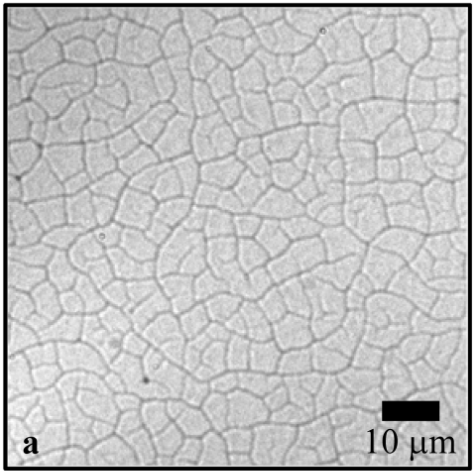 But none of the “mudcracks” I’ve seen appear to show the disconnected, fractured structure shown in this sample.
Overall, I’m still not very clear on what exactly the material used is, of if there are trenches/other features under this fractured layer. If you have any thoughts please comment below! I’m also planning to pick up a BMP280 and see is it essentially the same device, without the top die.