Today I decided to get the AFM I have here up and running. I’ve not had any formal training on an AFM (Atomic Force Microscope) so I’m feeling my way as I go. As a first test I wanted to try something with quite large feature sizes, I had no calibration standard so acquired some used wafers (in this case a late 90s FPGA (ProASIC)) with relatively large features as an initial test.
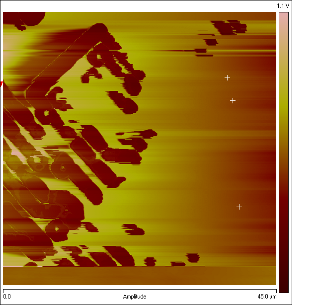
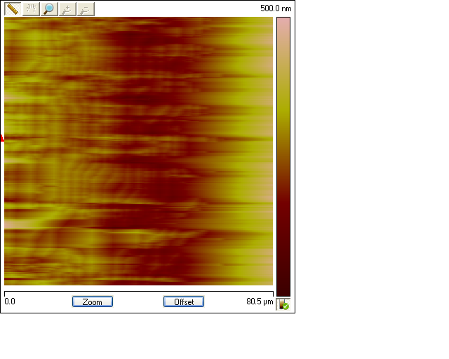
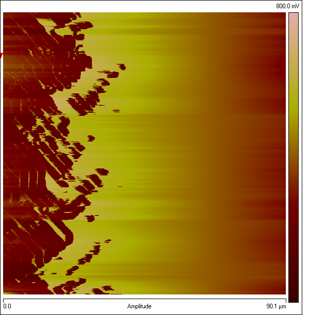
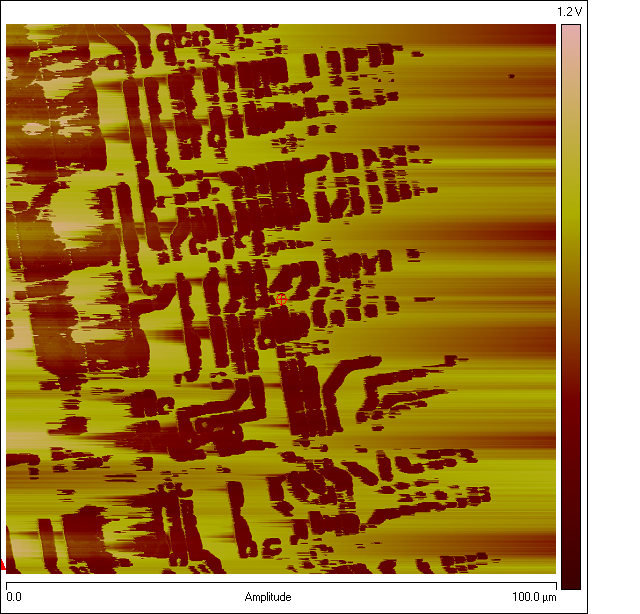
The image above shows some of the features I assume on the upper metal layer of the FPGA. The feature size seems to be around 200 to 700nm which seems about right for 90s tech. Cantilever installation, laser alignment and the imaging process is non-trivial. The videos below document the process I used to get these images:
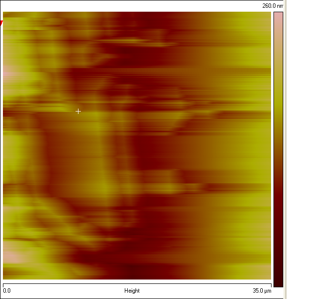
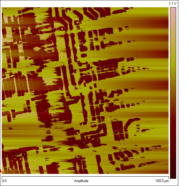
These two images were taken in “height” mode. They didn’t come out very well to my mind. It seems that switching the imaged value to “amplitude” (amplitude of what if not effective height I don’t know) seemed to produce much better images like that shown above.
The video above shows my test tentative experiments using the Axopatch 200A and a micropipette pulled using the Sutter P-97 as I described yesterday.
I used KCL diluted to ~100mM and sucked the solution into the pipette using a syringe. I didn’t have the correct tubing and pulled the sheath off a piece of silicon sheathed wire. It seemed to work ok. Drawing fluid into the pipette wasn’t easy I think I either have the wrong clamp for the pipette or perhaps it needs some PTFE tape to seal it.
Anyway, it appeared to more or less work and I could vary the current through the solution by changing the bias voltage. This is all I wanted for a first test and I now have a short list of bits and pieces I’d need to acquire to go further.
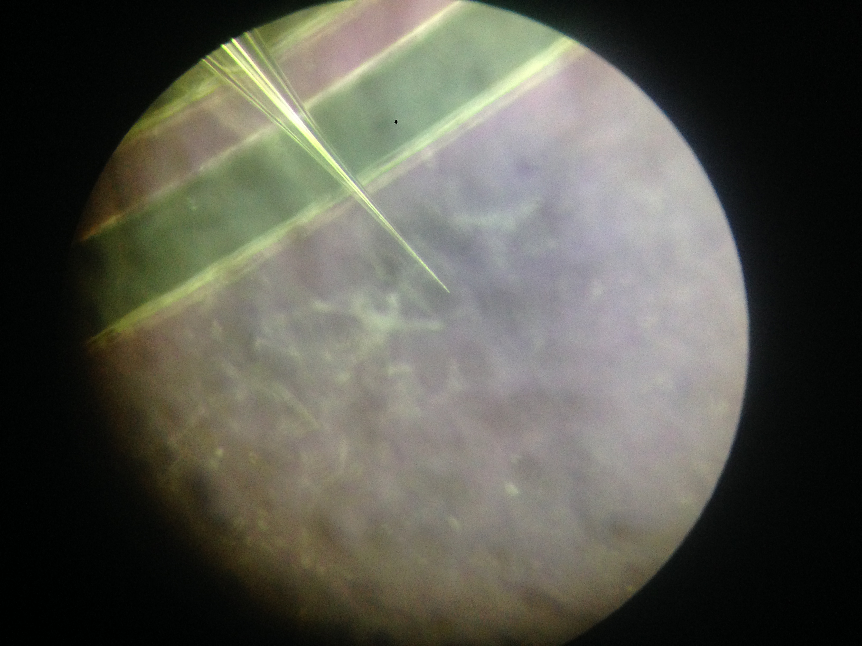
Today I tried out the pipette puller I picked up a few months ago. I figured it might be non-functional or need a new filament at least. But it seems to work well, a bargain considering I picked it up for a few hundred pounds and it goes for much more on eBay (and cost a few thousand new I believe).
Anyway, I could successfully pull pipettes as shown in the video above and pictured below. Next I might try some ionic current experiments to characterize the aperture.
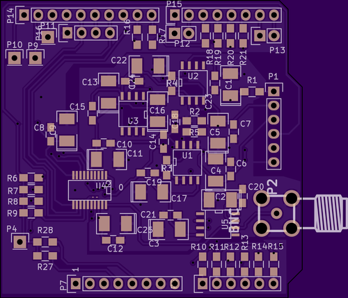
The previous revision of the AD5791 board worked well, however after reading this analog whitepaper on the ad5791 I decided to change the routing. I split out the ground planes so the board is more clearly divided into analogue and digital sections now. I really need to figure out how to correctly measure the noise on the output, but at some point it would be useful to benchmark the designs for noise. As always Kicad files and gerbers are linked below:
My name is Nava Whiteford. I’ve worked for a few sequencing companies. I have equity in a few sequencing companies based on my previous employment (I try to be unbiased in my posts). You can contact me at: [email protected]