I’ve been playing with a multislope ADC design. Multislope ADC are often used in high end multimeters, and as I have a mild obsession with 8.5 digit multimeters, I wanted to try making a multislope ADC. The current design, such as it is was developed with significant input from EEVBlog users (see this thread).
This post documents initial bring up and tests of the first revision of the PCB. Links to Kicad files, and data used in plots can be found at the end of this post.
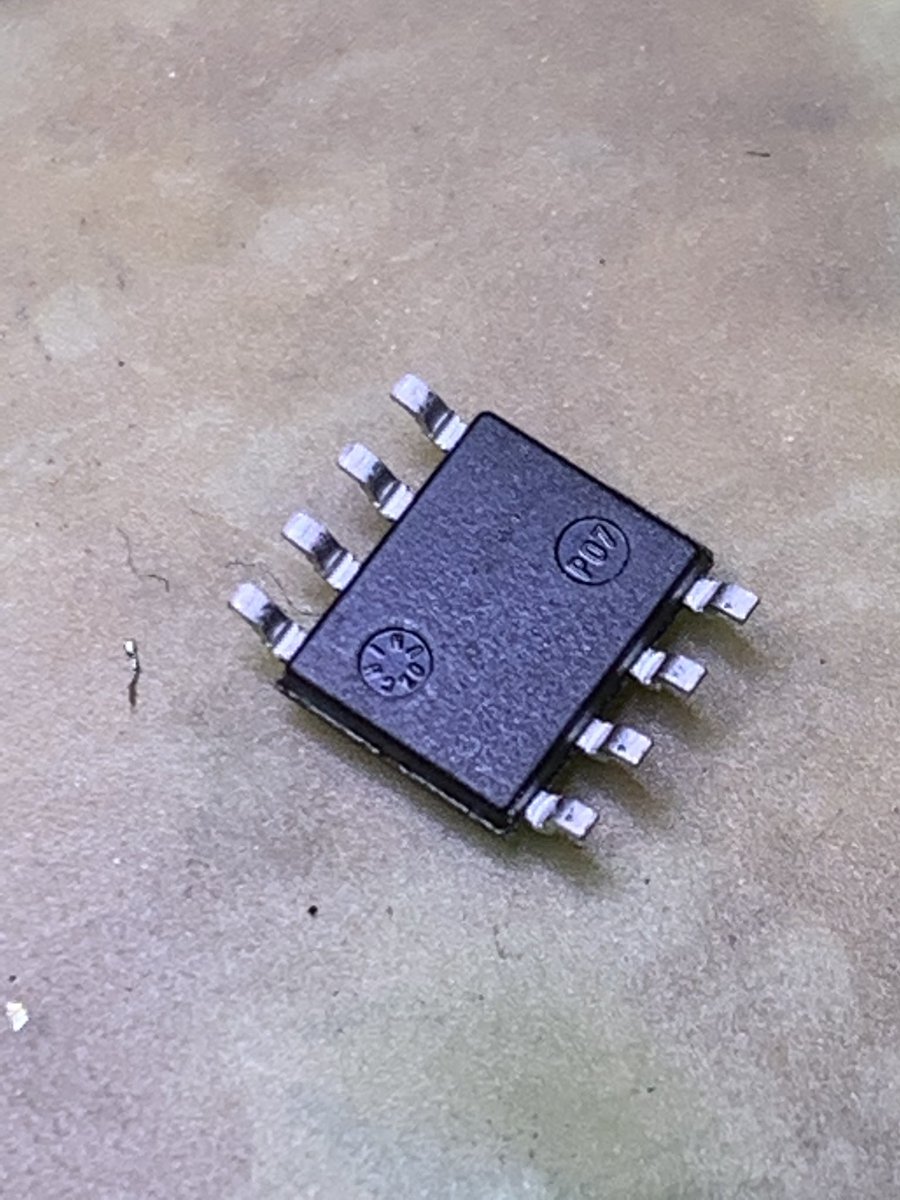
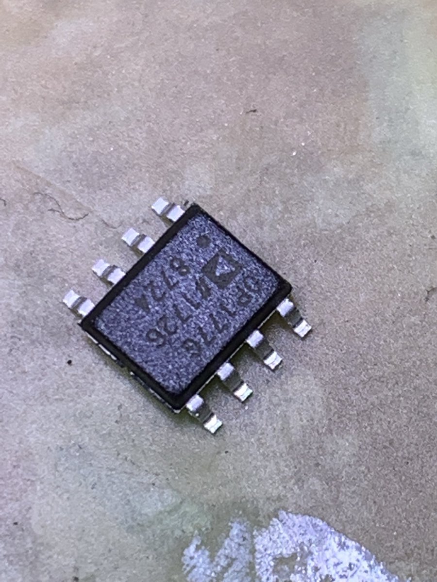
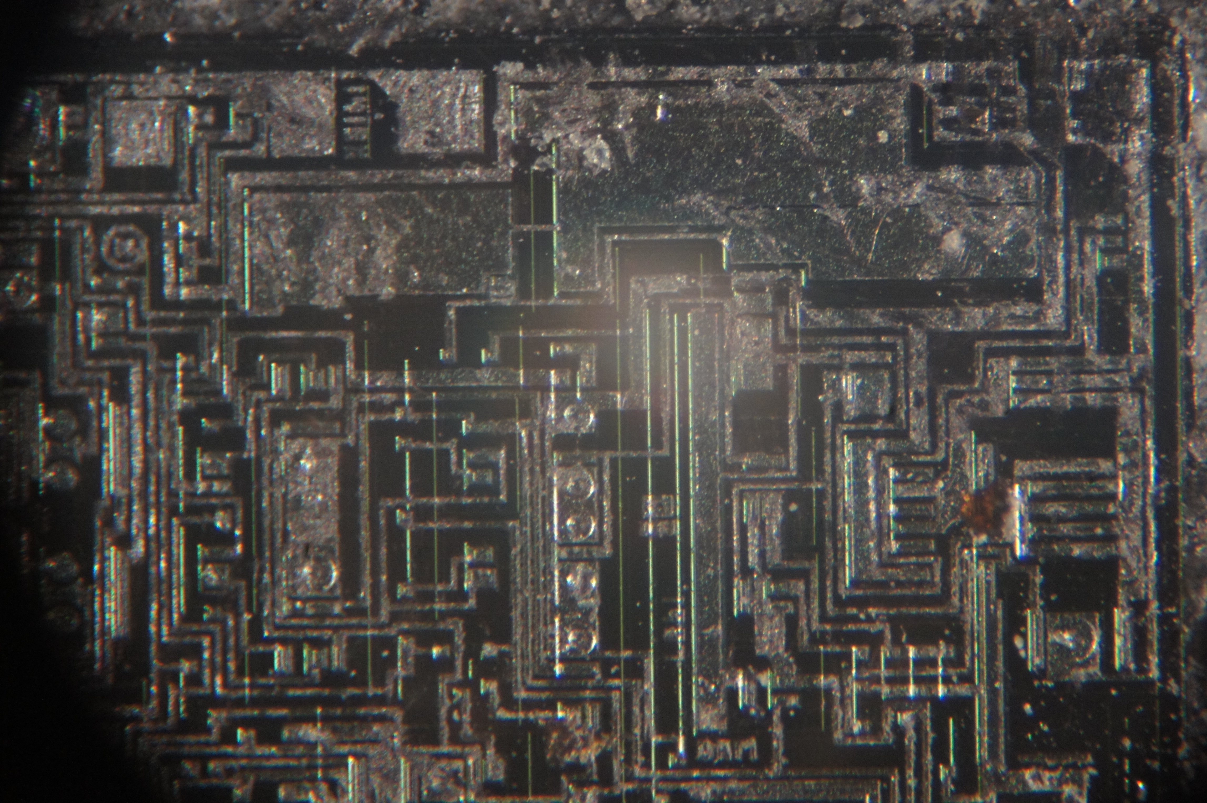
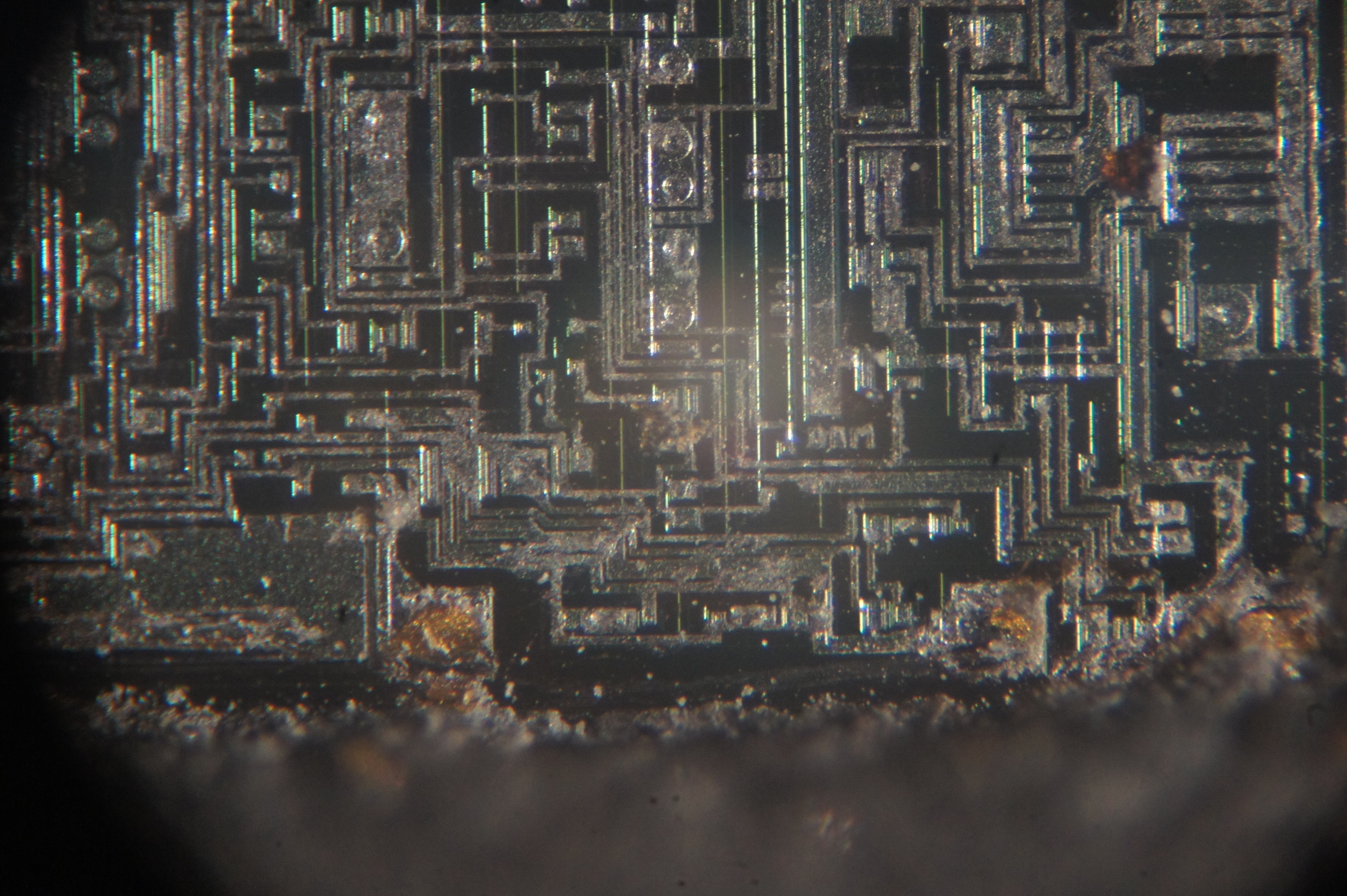
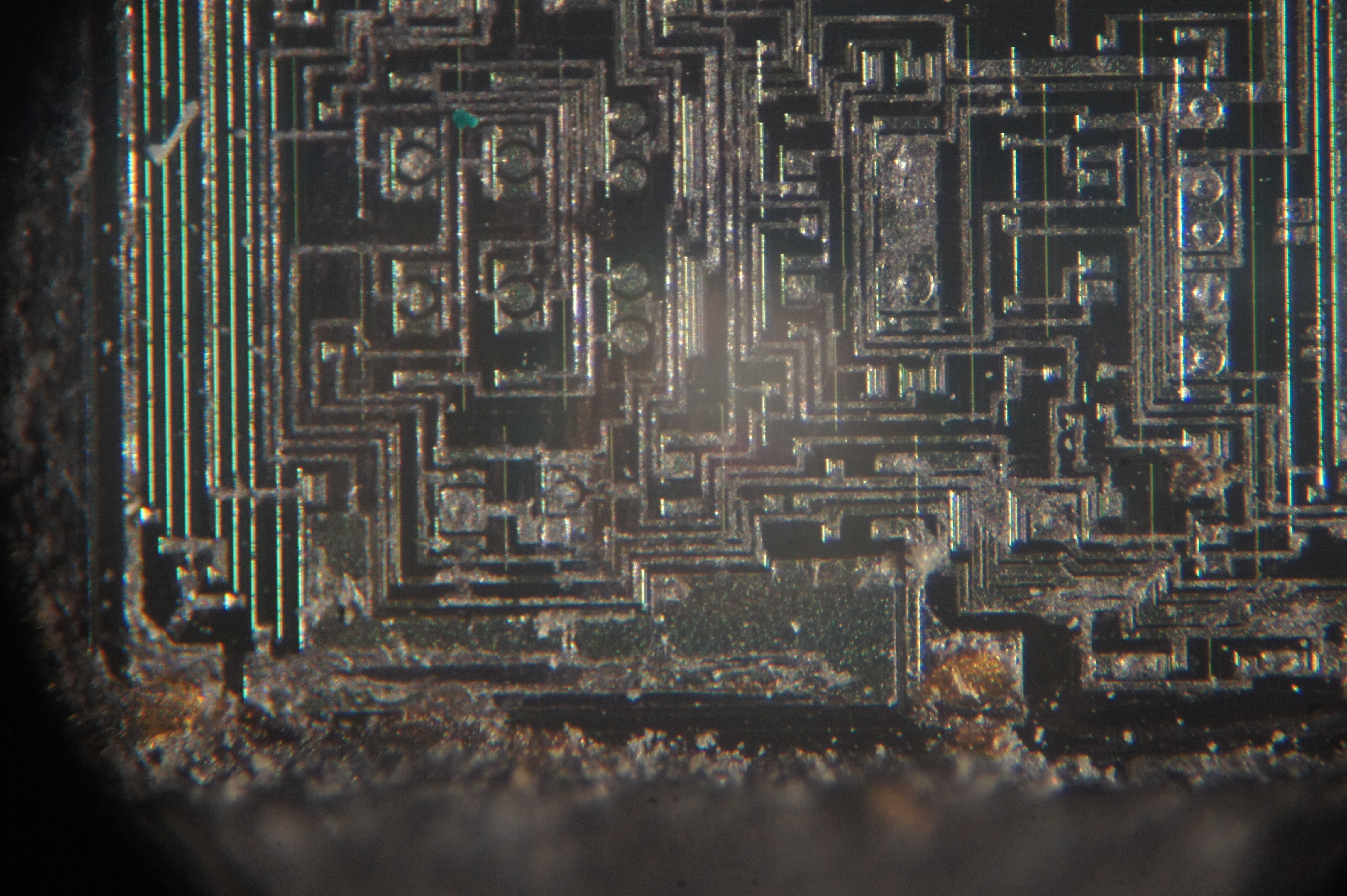
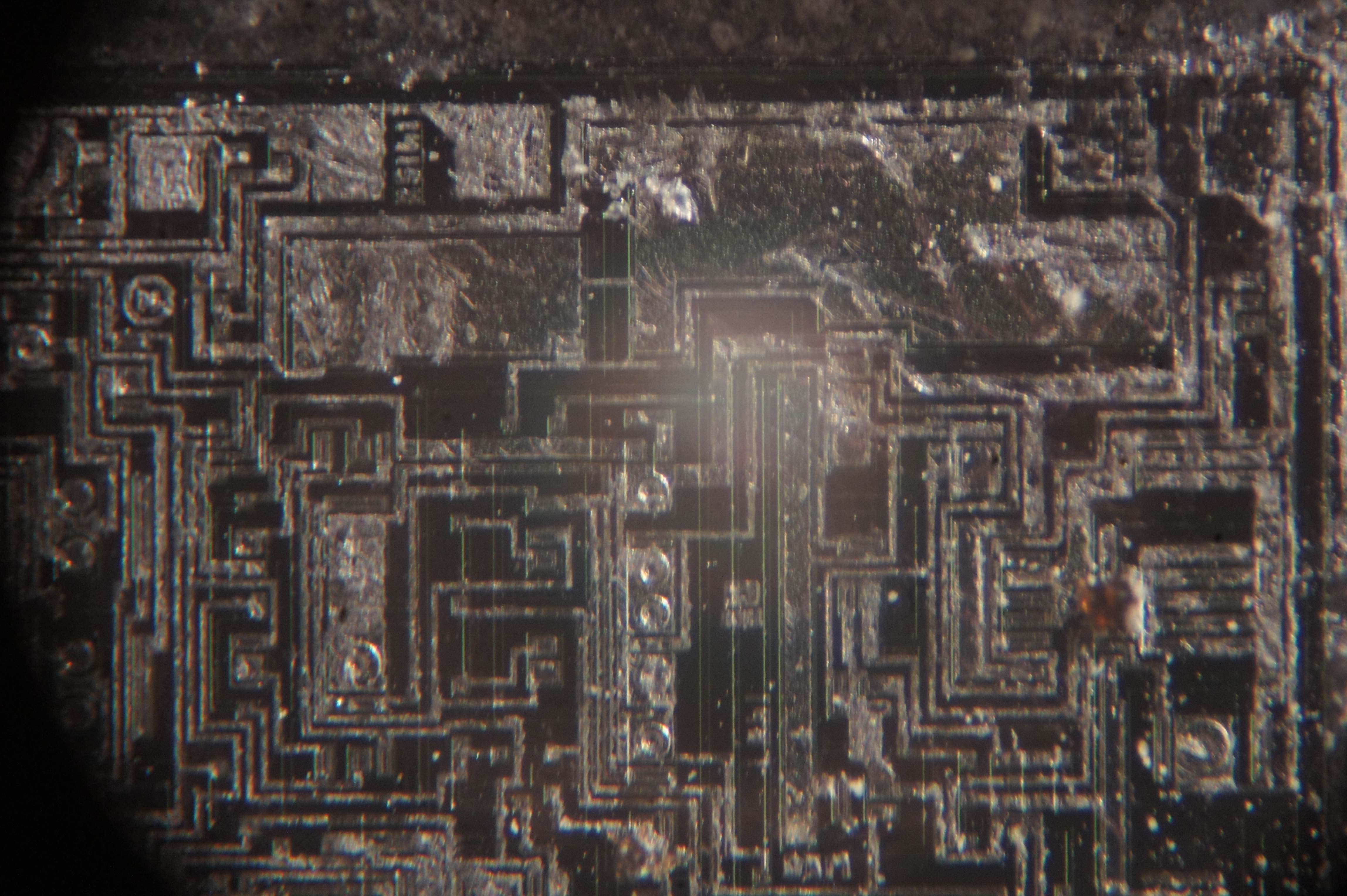
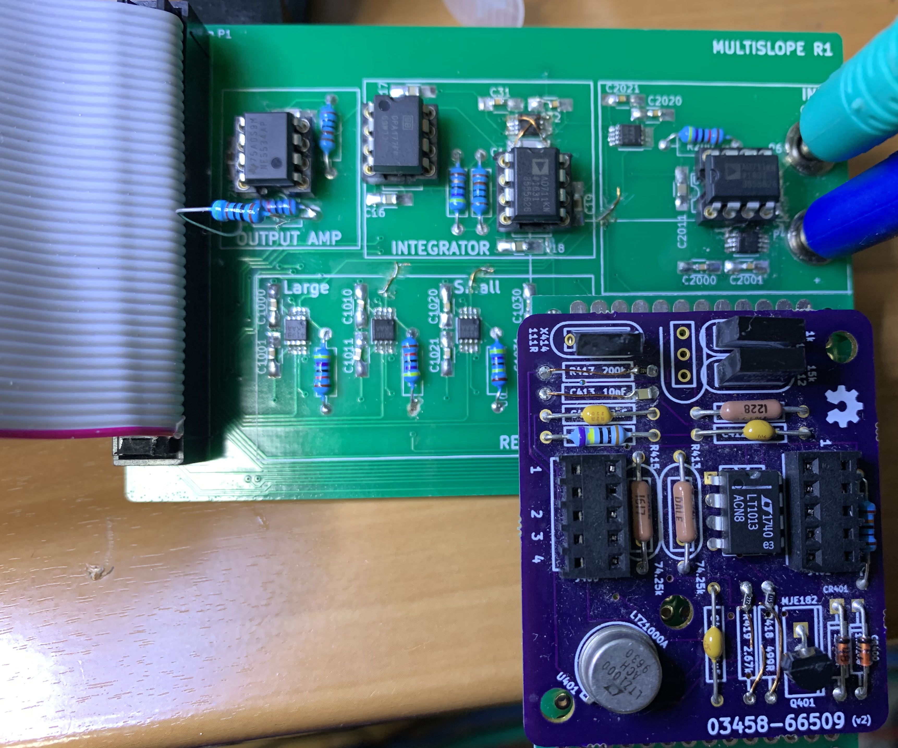
Components used in this test
All resistors are standard, cheap 1/4 Watt metal film resistors. The large slopes are 47K. Small slopes 4.7M. The input resistor (R200) is also 47K.
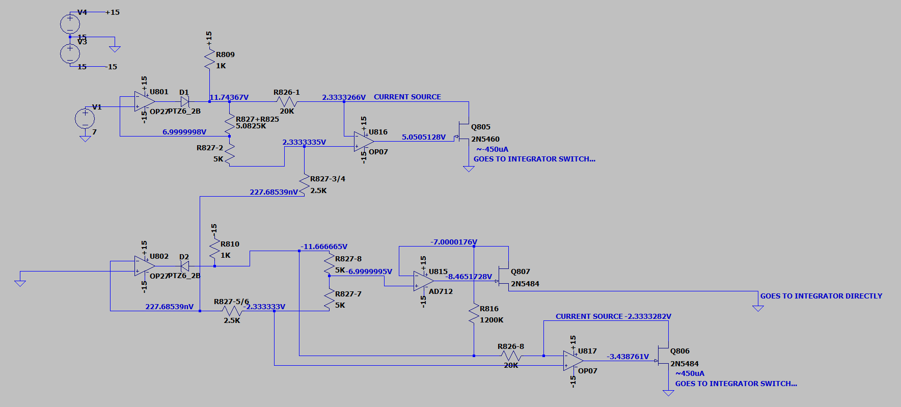
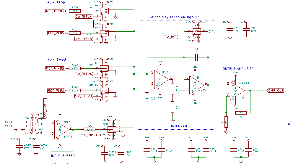
The design uses a 2 opamp integrator. Notionally this allows you to combine an opamp with good low frequency response with one with good high frequency response. A voltage divider sits between the two opamps. R9 is 47Ohm, R8 1K.
On the output amplifier R3 is 1K and R7 is 470Ohm to give a gain of ~0.5. This allows the Arduino Mega which I’m using to control the amplifier to read almost the full positive range of the integrator output (12V).
The integrator capacitor is an NP0 10nF, Murata GRM3195C1E103JA01D.
The switches are all DG419s. This includes the part marked DG417 on the schematic, which resets the integrator. All the DG419s are Vishay DG419Bs MSOP8s, except for the integrator which uses an Analog ADG1419BRMZ (I ran out of Vishay DG419s). Update: I attempted to rebuild this circuit using only ADG1419BRMZ, it did not work well. My guess is that there is too much charge injection… charge injection is not listed in the datasheets…
I’m using a LTZ1000 reference to supply the slopes. This sits on an 3458A A9 PCB. I’m using a A9 clone from here.
All opamps are socketed. In this test I used a NE5534 on the output. An OPA177 and AD711 for the integrator, an AD711 on the input, and an LT1013 to buffer/invert the reference voltage.
Build Issues
There were a few errors in the schematic and layout. These include:
- The banana plug holes are too small for the sockets.
- The output opamp connected incorrectly (power swapped)
- The input opamp was connected incorrectly (I forget the exact issue).
- The reference voltage buffer/inverter was wired incorrectly.
- The reference PCB covers the banana plugs when installed.
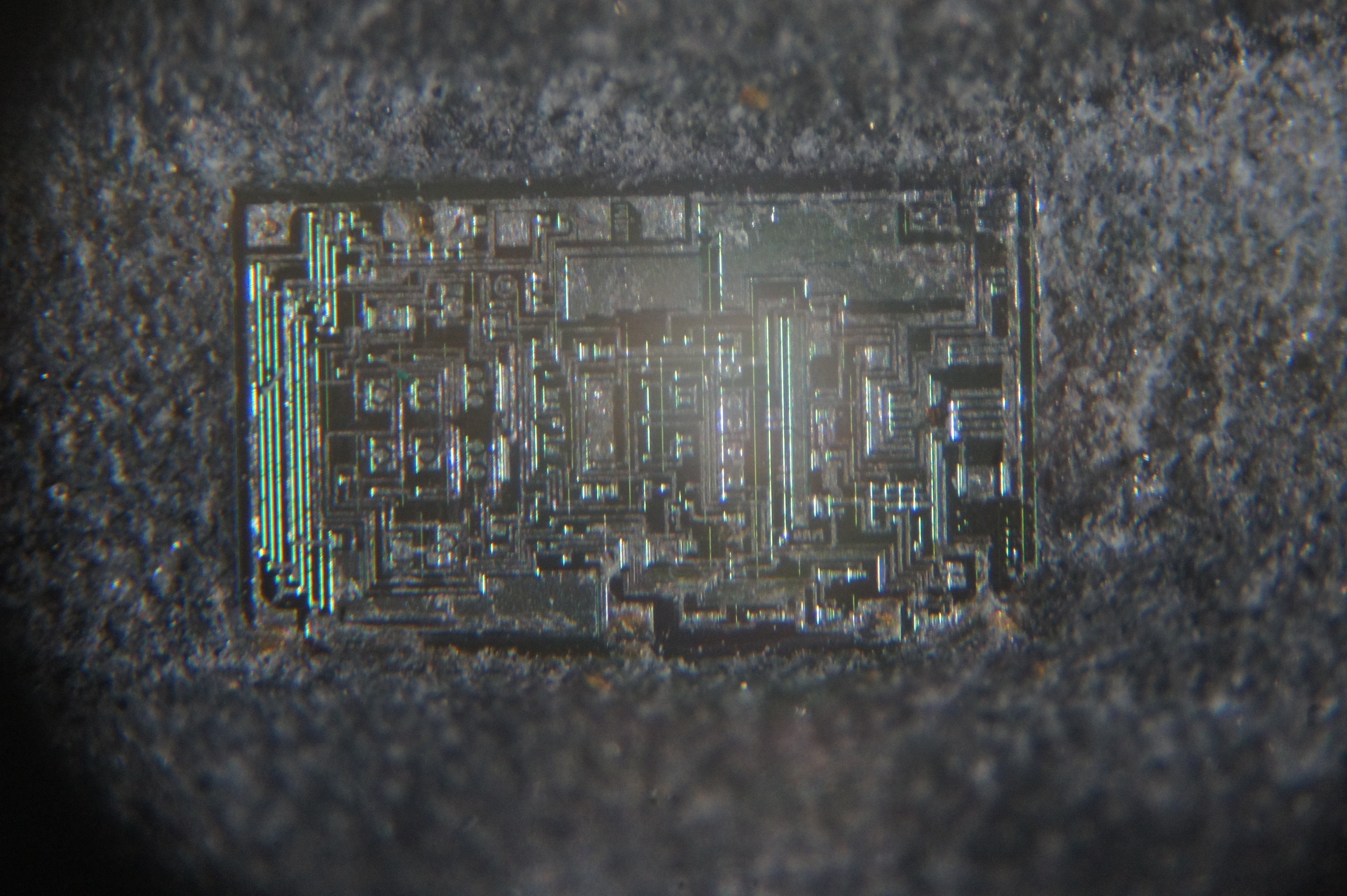
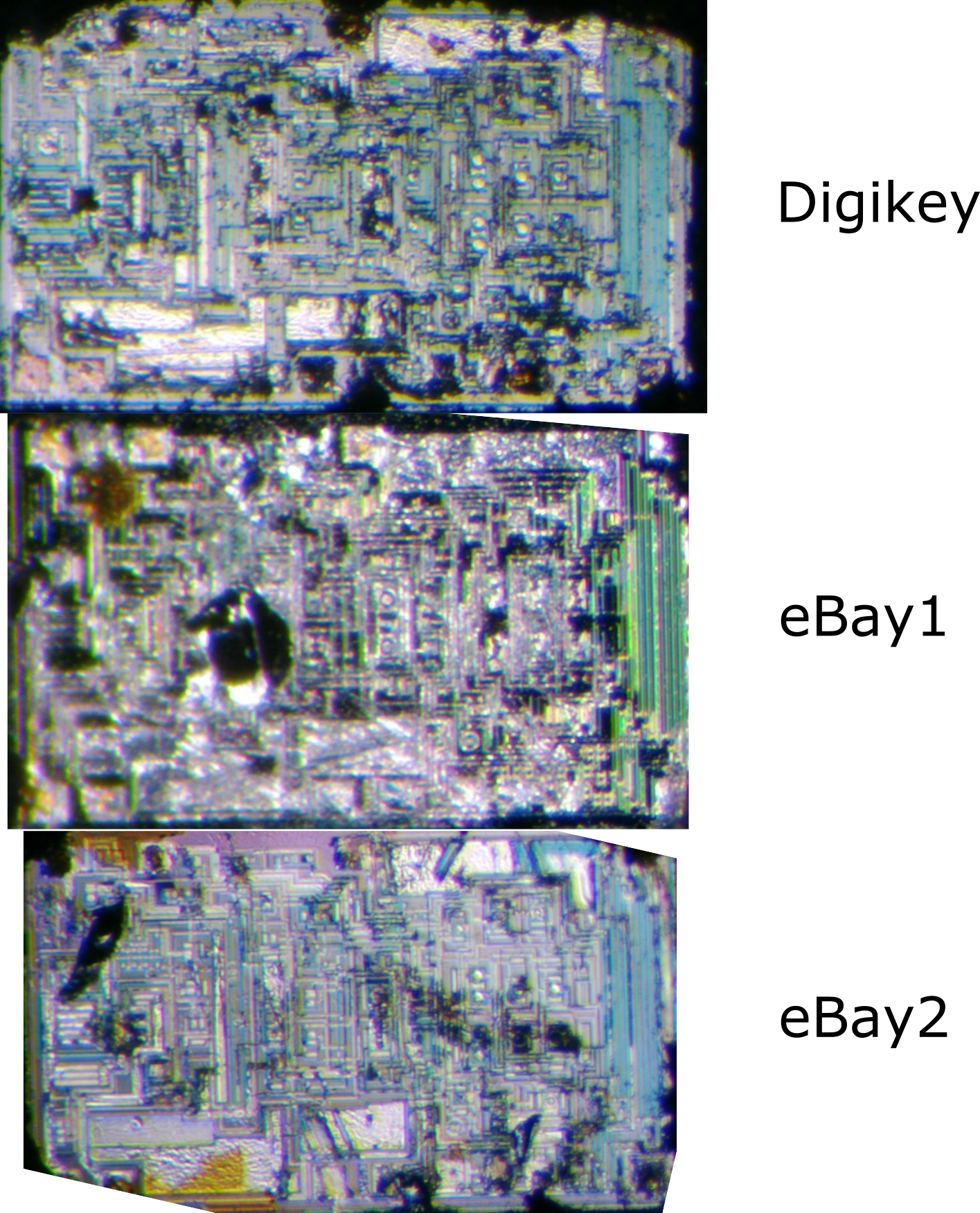
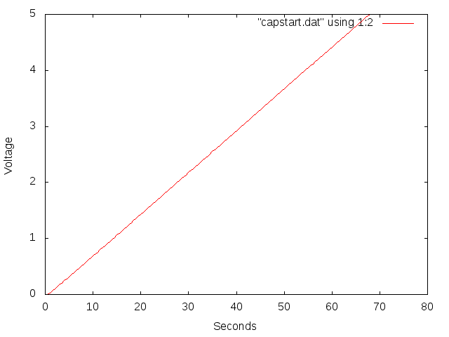
These should be resolved in the schematic, but I’ve not fixed the layout yet. In the build you’ll also notice that I’ve hacked around with other parts of the PCB too. This was when I was cutting traces to try and figure out where leakage current was coming from and charging the integration capacitor. In the end this seemed to be coming from flux I couldn’t clean from under the DG419 switches. I removed, cleaned and replaced these, being more conservative with my usage of flux when re-soldering them. This removed most of the leakage current.
Initial tests
When I first brought up the design there was a lot of charge accumulating on the integrator after reset without any of the slopes or the input connected. After about 3 seconds the integrator would rise to the rail voltage (12v). After some investigation, this seemed to be caused by excess flux remaining under the DG419s. After cleaning this out, it takes ~60 seconds for the integrator to charge to the rail voltage. The following plot shows the output as recorded by an Arduino analog input:
I’ve written code to drive the ADC board in a basic dual slope configuration. This works for bother the large and small slopes. In the tests below however I’m using the small slopes only. Arduino code is provided in the notes at the end of this post.
The tests use a DP832 to supply rail voltages (+/- 12 and 5V). A 33220A function generator is used to generate the input (this is probably not particularly low noise/accurate).
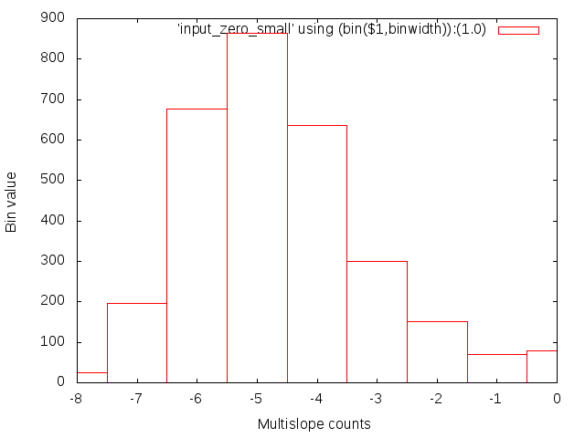
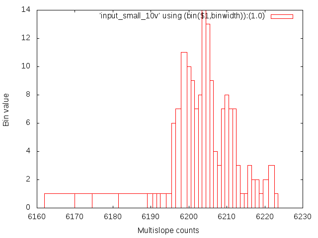
The following plot shows a histogram of ADC counts when the input is zero:
And here at 10V:
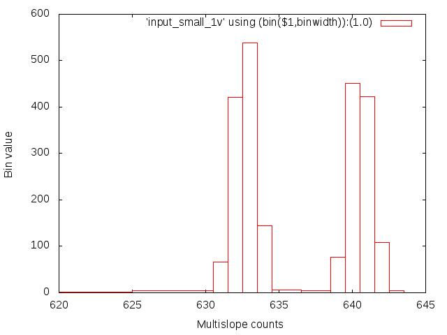
There’s something weird going on, as in some cases the histogram is bimodal. For example here at 1V:
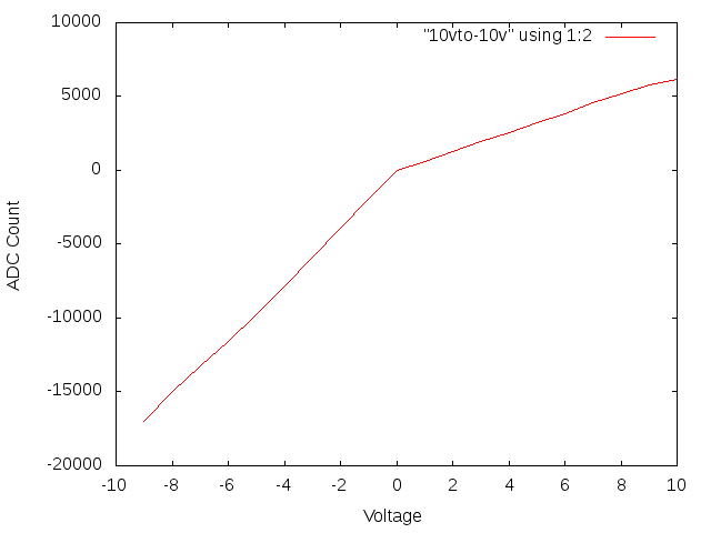
Integration of positive voltages is also about 3 times quicker than negative voltages. It’s not clear to me why this is. Positive and negative voltages use different reference resistors, however these don’t seem to be significantly different and I need to investigate further.
The positive and negative responses however seem to be quite linear. The following plot shows input voltage versus ADC count. You can see the slope difference between positive and negative voltages quite clearly:
Before moving forward, I’d like to better understand why I’m seeing this difference between positive and negative voltages. I should then be in a position to combine large and small slopes to create a multislope ADC.
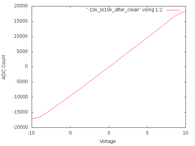
Update: I cleaned the board in an ultrasonic cleaner (distiled water, 60 degrees for ~15min, with a small amount of washing up liquid. Then agitated in IPA for ~30min). This seems to have cleared up the slope issue above. Here’s a revised graph:
Notes
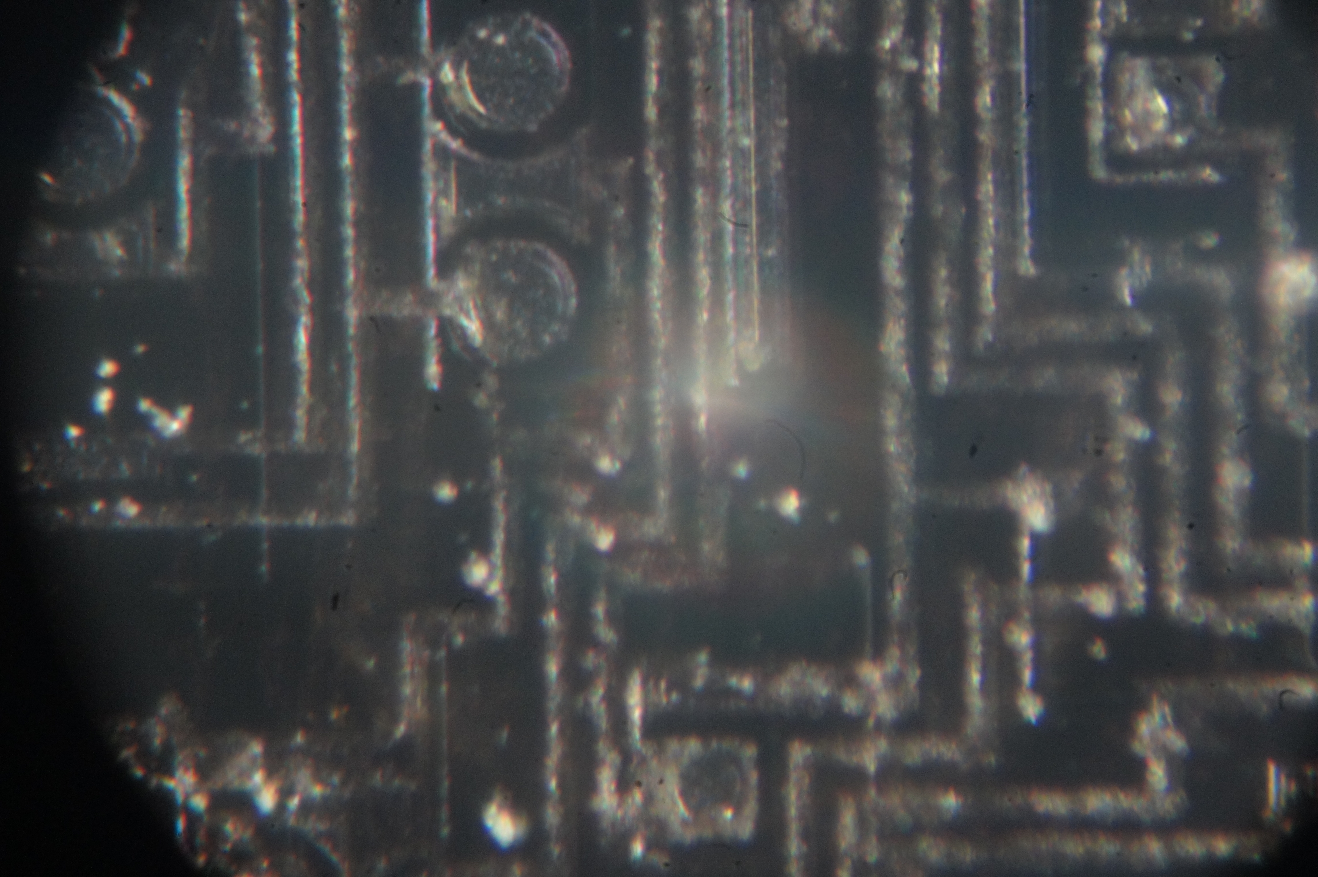
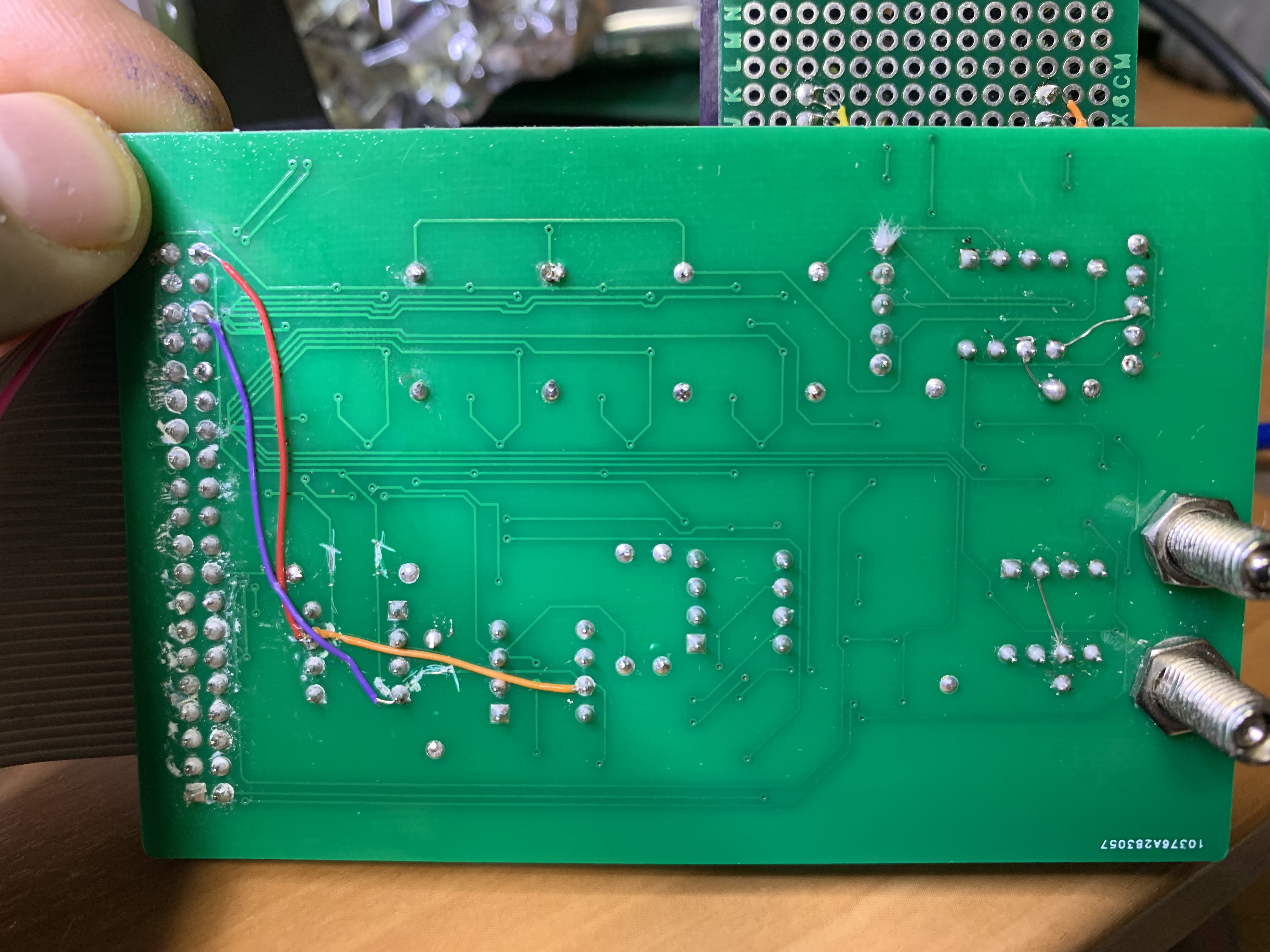
PCB Back:
EEV Blog Thread
Data for plots
Kicad files
Hacky code used in this post:
#include <SPI.h>
// name header arduino
// SW_RST 2 4
// SW_INPUT2 6 3
// SW_INPUT1 8 2
// SW_REF2B 10 A7
// SW_REF2A 12 A6
// SW_REF1B 14 A5
// SW_REF1A 16 A4
// CMP_OUT 18 A3
#define SW_RST 5
#define SW_INPUT2 3
#define SW_INPUT1 2
#define SW_REF2B A7
#define SW_REF2A A6
//#define SW_REF1B A5 - original
#define SW_REF1B A1
#define SW_REF1A A4
//#define CMP_OUT A3 - original
#define CMP_OUT A2
void input_off() {
digitalWrite(SW_INPUT2,HIGH);
delayMicroseconds(100);
digitalWrite(SW_INPUT1,LOW);
}
void input_on() {
digitalWrite(SW_INPUT1,HIGH);
delayMicroseconds(100);
digitalWrite(SW_INPUT2,LOW);
}
void references_off() {
digitalWrite(SW_REF1A,HIGH);
digitalWrite(SW_REF1B,HIGH);
digitalWrite(SW_REF2A,HIGH);
digitalWrite(SW_REF2B,HIGH);
}
int read_cmp() {
int r = analogRead(CMP_OUT);
return r;
}
void dump_cmp() {
int r = read_cmp();
Serial.print(r);
Serial.print(&amp;amp;quot; &amp;amp;quot;);
}
void ref_on(int p) {
digitalWrite(p,LOW);
}
void ref_off(int p) {
digitalWrite(p,HIGH);
}
void reset_integrator() {
digitalWrite(SW_RST,HIGH);
delayMicroseconds(10001);
// delay(3000);
digitalWrite(SW_RST,LOW);
}
void setup() {
// put your setup code here, to run once:
Serial.begin(115200);
pinMode(SW_RST ,OUTPUT);
pinMode(SW_INPUT2,OUTPUT);
pinMode(SW_INPUT1,OUTPUT);
pinMode(SW_REF2B ,OUTPUT);
pinMode(SW_REF2A ,OUTPUT);
pinMode(SW_REF1B ,OUTPUT);
pinMode(SW_REF1A ,OUTPUT);
pinMode(CMP_OUT ,INPUT );
input_off();
references_off();
reset_integrator();
// ref_on(SW_REF2B);
Serial.println("input complete");
for(;Serial.available() == 0;) {
dump_cmp();
Serial.println();
delay(500);
}
Serial.println("running...");
}
void loop() {
// Serial.println("start");
input_off();
delayMicroseconds(1000);
// Serial.println("inputoff");
references_off();
// Serial.println("refoff");
delayMicroseconds(1000);
reset_integrator();
// Serial.println("int reset");
delayMicroseconds(1000);
int p = read_cmp();
int c=0;
for(;p != 0;) {
reset_integrator();
p = read_cmp();
//Serial.print(p);
//Serial.print(" ");
c++;
if(c>10) break;
}
//Serial.println();
//dump_cmp();
input_on();
delayMicroseconds(500);
input_off();
int pol = read_cmp();
// input negative
if(pol &amp;amp;gt; 0) {
Serial.print("-");
unsigned int count=0;
for(;;) {
ref_on(SW_REF2B);
delayMicroseconds(5);
ref_off(SW_REF2B);
int c = read_cmp();
if(c == 0) break;
count++;
if(count > 64000) {Serial.print("B"); count=0;}
}
Serial.println(count);
}
// input positive
if(pol >= 0) {
Serial.print("+");
unsigned int count=0;
for(;;) {
ref_on(SW_REF2A);
delayMicroseconds(5);
ref_off(SW_REF2A);
int c = read_cmp();
if(c > 0) break;
count++;
if(count > 64000) {Serial.print("B"); count=0;}
}
Serial.println(count);
}
}