Archive for the ‘Uncategorized’ Category.

Sputtering machine notes

Sputtering machines (also called sputter coaters) are amazing, they’re able to lay down thin films of both conductive and insulating material.

Somewhat surprisingly for such an advanced technique, sputtering has been known about for a long time, though it’s mechanism was not originally well understood.

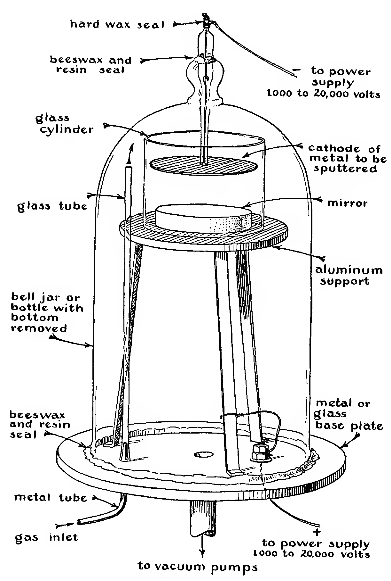
John Strong’s excellent 1920s book “Procedures in Experimental Physics” for example includes this great diagram of a sputtering setup:

sputtering_procedures

The procedure hasn’t changed much since then, and I’ll use this diagram as a reference. As you can see in the diagram the metal to be sputtered (commonly and slightly confusingly called the target) cathode is connected to a large negative voltage typically in-excess of 1000volts. The material to be coated is placed near the target. In this diagram a piece of glass is being coated with metal to make a mirror, a fairly typical application of sputtering. Behind the material to be coated is a metal plate which is grounded with respect to the negative supply.

Sputtering will not work in air, so the whole process takes place in a vacuum chamber. It is however not a particularly high vacuum, and I believe only a roughing pump is required. The process actually requires gas to be present in the chamber. Typically argon, but other noble gases or even air can be used.

In the sputtering process electrons leave the target which is negatively charged, and move toward the substrate. Very occasionally as they follow this path, they hit an atom of gas. This ionizes the gas atom. The now positively charged atom is drawn toward the target material and smashes into it. This process smashes single atoms off the target which fly out into the vacuum, eventually hitting the substrate to which they anneal.

This is the basic process. Sputtering has a number of advantages over vapor based deposition techniques (which boil a metal in a vacuum in order to eject atoms into the vacuum and then onto the substrate). And as we will see, can even be used to generate films of insulating materials.

DC Sputtering

The process described above is basic DC sputtering. While this was the original technique there is one refinement which practically all sputtering machines now use. This is to confine the electrons somewhat using a magnetron. The magnetron uses magnetic and electric fields to keep the electrons near the target.

dcputtering

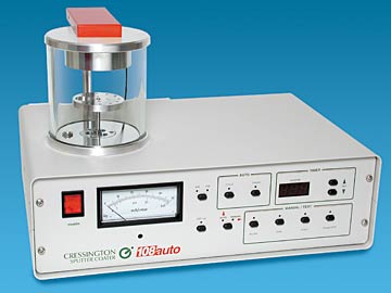
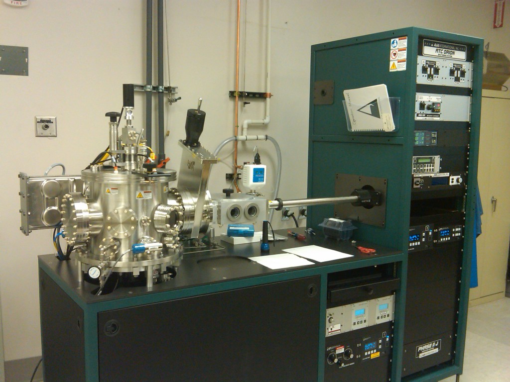
The above image shows a typical DC Magnetron sputtering machine. These typically cost a few thousand USD used. Their most common application is in coating samples prior to being imaged in an SEM. SEMs in general require samples to have a conductive outer layer.

RF Sputtering

rfsputter

RF Magnetron Sputtering machines tend to be a bit more serious, like the one shown above. There’s no real reason that they need to be that big however. RF machines use an AC, rather than a DC voltage. Typically these systems operate at a frequency of 13.56MHz. An AC voltage means that the target wont build up any charge, allowing insulting targets to be used.

Self builds

A number of people have built their own sputtering machines from parts, notably Ben Krasnow has an excellent video on his build:

Other builds are a little more ghetto, but interesting because they often re-use microwave parts to build the magnetron:

Imaging of Rice – A review

Yesterday I went with some friends and looked at a SEM we’re thinking of buying. We’d likely keep it in a hackerspace located in a local rice farming community.

This naturally got me thinking about imaging rice, and I thought I’d take a quick look at what’s already been done.

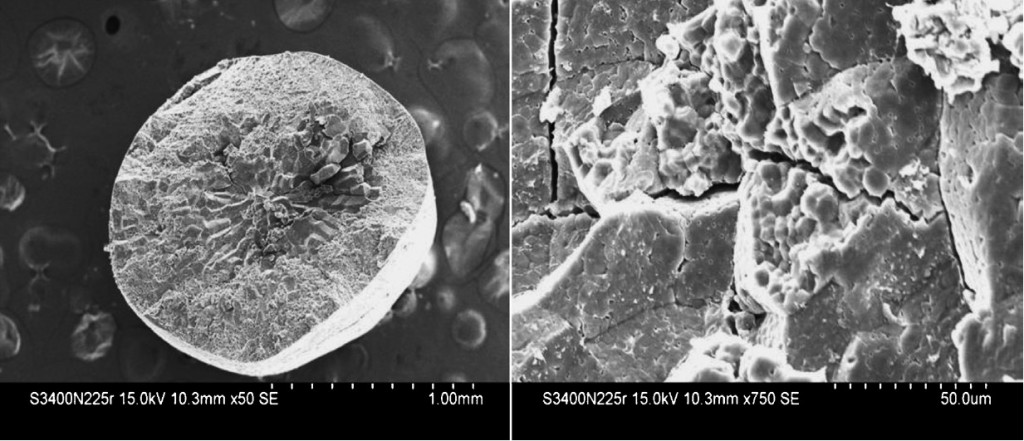
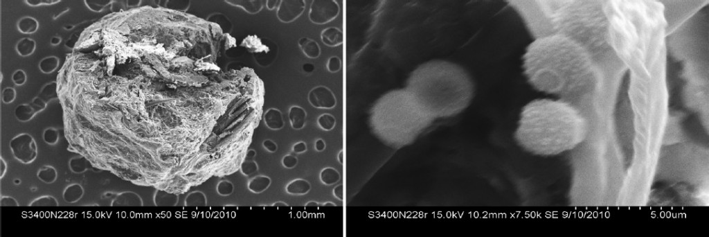
This first article is concerned with Alfatoxin contamination in rice. Alfatoxins, produced by a fungus is a carcinogen, and can also produce liver failure. This first study was looking at normal and damaged rice grains, to identify the presence of the Alfatoxin producing fungi A. flavus. In conclusion, they have some cool images of normal and damaged rice, and fungal spores:

normalrice
damagedrice [3]

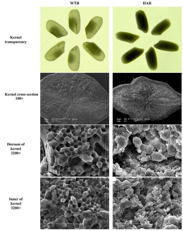
A second study looked at wild-type and genetically modified high-amylose rice. High-amylose rice is potentially better for diabetics. The study seems to have no specific goal, but just characterizes the two rice types. The methods section was interesting, and mentions their experimental rice field (never before have I wanted an experimental rice field, now I do). The prep process is basically as follows:

  1. Air-dry, and dehusked in an electrical dehusker (model SDL-A)
  2. Polish using a grain polisher (Model Kett, Tokyo, Japan)
  3. Dry samples in an oven a 40°C for 12 hours.
  4. Cool samples in a dessicator.
  5. Sputter coat with gold palladium.

The resulting images clearly show the large scale differences between the two rice types:

ricestm1
[1]

The final study isn’t using SEM imaging. Rather they use MRI and micro-CT imaging to look at the internal structure of the rice as it cook. The abstract of this paper is awesome:

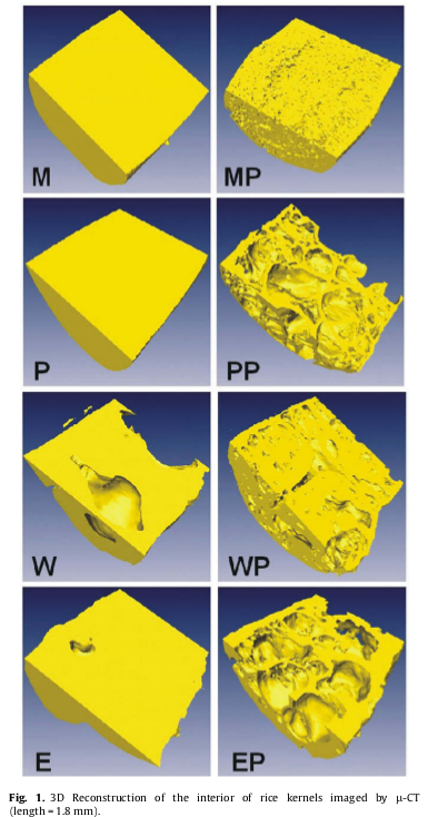
In order to establish the underlying structure-dependent principles of instant cooking rice, a detailed investigation was carried out on rice kernels that were processed in eight different manners. Milling, parboiling, wet-processing and extrusion were applied, with and without a subsequent puffing treatment. The mesostructure of the rice kernels was examined by DSC and XRD, and the microstructure by micro-CT. Hydration behaviour during cooking was studied by MRI in a real-time manner. Based on simple descriptive models, three different classes of cooking behaviour can be discerned. The water ingress profiles during cooking of these three classes matched well with simulations from a model that was based on water demand of the starch mass and the porous microstructure of the kernels. Thus a clear correlation between meso/microstructure of a rice kernel and the cooking behaviour has been established.

riceuct [2]

  • M: Milled
  • P: Parboiled
  • W: Wet-processed
  • E: Extruded
  • MP: milled and puffed
  • PP: parboiled and puffed
  • WP: wet-processed and puffed
  • EP: extruded and puffed

Hmmmm I’d rather have a boil of extruded and puffed coated rice.

[1] Study of kernel structure of high-amylose and wild-type rice by X-ray microtomography and SEM>

[2] The effect of rice kernel microstructure on cooking behaviour: A combined
l -CT and MRI study

[3] Aflatoxin contamination in stored rice variety PAU 201 collected from Punjab, India

Visit to see a SEM (electron microscope)

photo 1

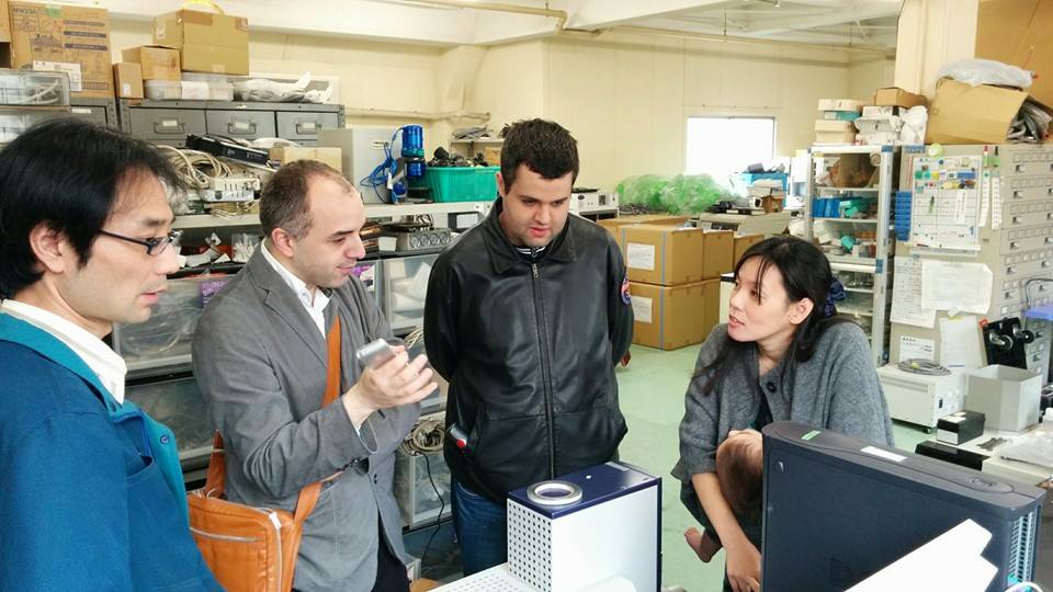
Today I went with some friends, my wife and 8 month old baby to see a SEM. We’re planning to buy one for shared use at a local hacker space (here in Japan).

semlook

I’m the balding one, wearing a jacket and trying to look like I should be allowed to own an SEM.

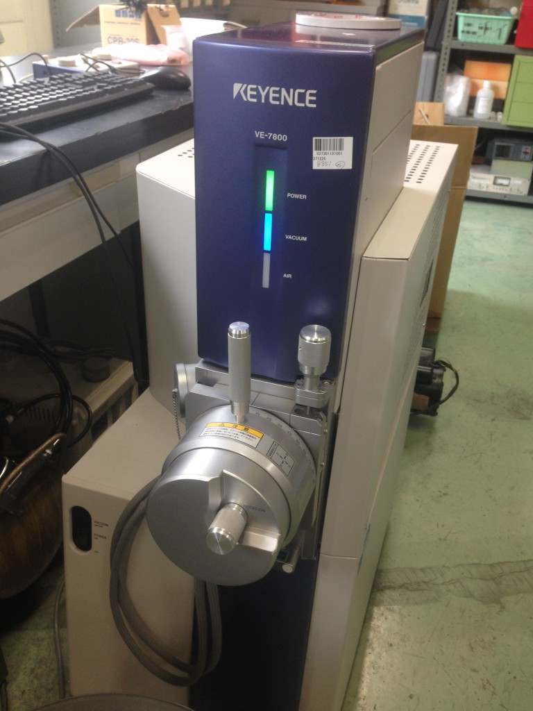
The instrument bears little relation to the SEMs of old, or even the models from the 60s and 70s, it’s a ~2003 era instrument billed as a “deskside SEM”. Unfortunately, as far as I know, it’s only available in Japan. The device we looked at is similar to these current models.

photo 1(4)whitesuit

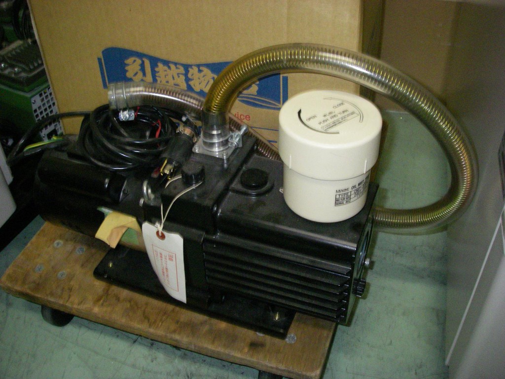
It’s also very quiet. SEMs operate at vacuum, and the unit uses as external roughing pump:roughingpump

As well as an integrated turbo molecular while compressors and turbo molecular pumps have a reputation for being somewhat noisy the instrument was very quiet in operation. We could easy see this being operated in a residential environment if required.

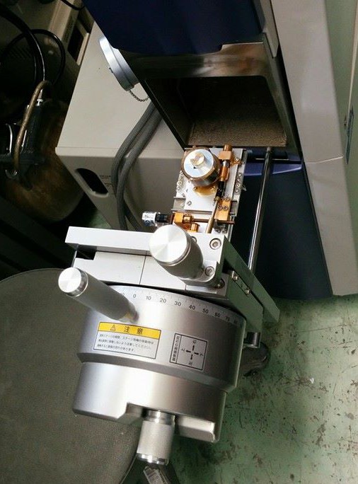
It’s also very easy to run a sample on this machine, it takes about 5 minutes for the vacuum to come up before imaging. Here’s the sample chamber:

photosem

I was concerned that there might be special mounting requirements, but the sample just sits on some (I assume conductive) tape. It can also take what I believe is a standard sample mount, but this isn’t required.

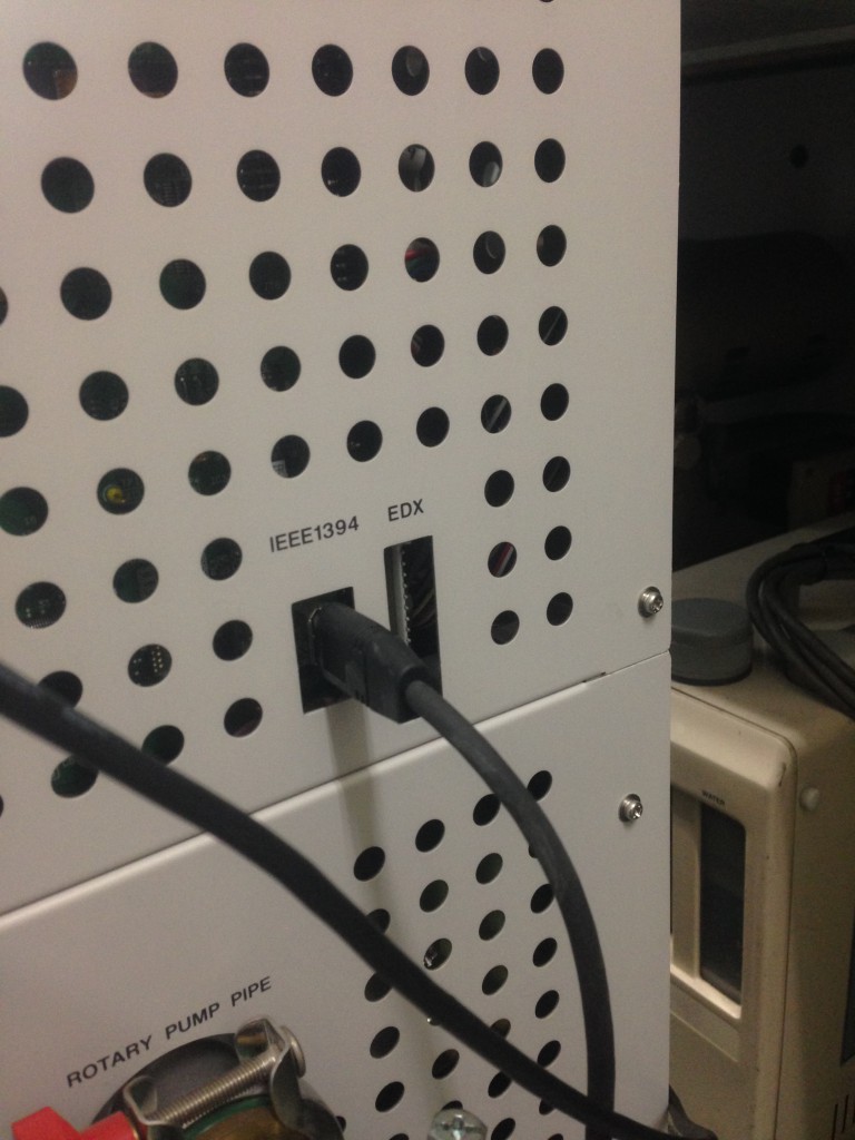
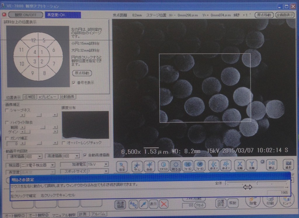
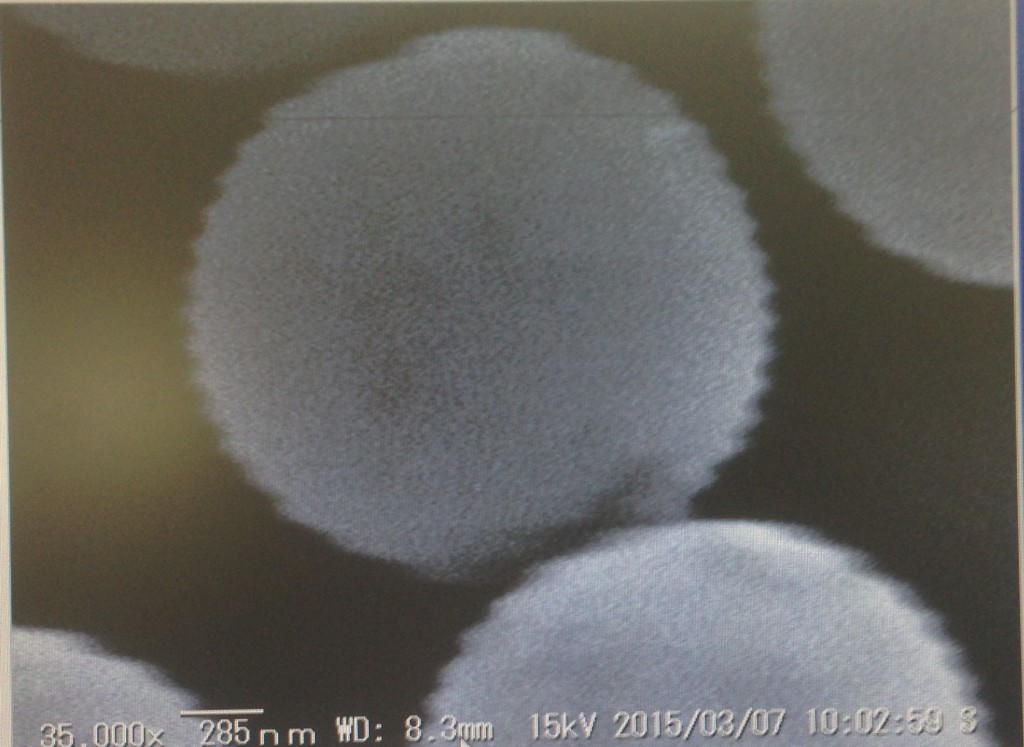
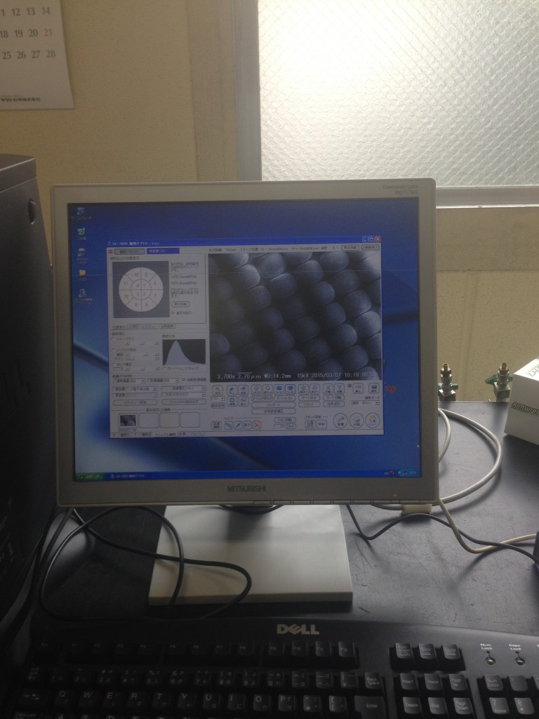
photo 2(4)The instrument interfaces to the device PC over Firewire and USB. The software on the PC is locked to the instrument via a license file. After poking around the machine it was onto imaging. We started while a sample provided by the salesman. He said this was gold sputtered on a surface, I wasn’t aware that gold balled up like this when sputtered. I think something was possibly lost in translation (please leave a comment or email me if you have some background here). They however did appear to be uniform spheres of ~1micron in diameter:

photo 1(6)

Here we are at 35000x:

photo 3(8)The instrument is vibration sensitive, and you can see some noise at this point (there was nearby construction going on which might have affected things). This vibrational noise was only present on this image, it went away pretty quickly, but we’ll be keeping this in mind when we setup the instrument.

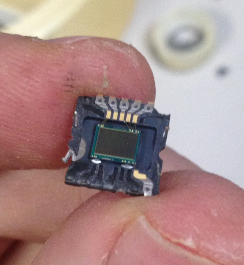
Now we’d confirmed that the machine was working we moved onto other samples, starting with the CCD IC I extracted yesterday. Here’s the chip again:

photo 5(1)

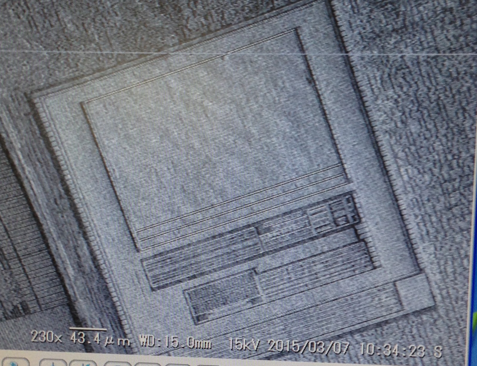
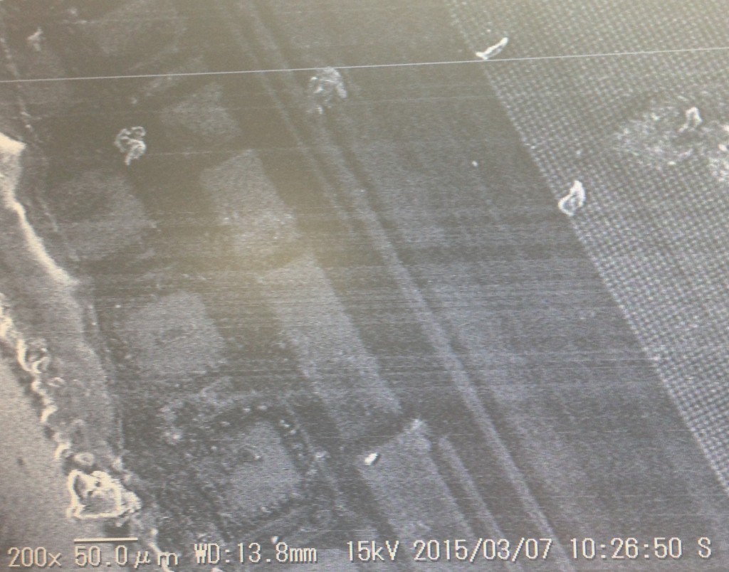
Under the SEM at x200:

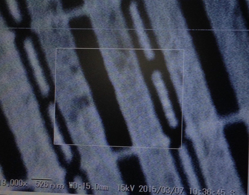
You can already get an idea of the feature sizes involved here. These is an old CCD and the lens on the right of the image are a few microns. I believe the bond pads are on the left, and between the two should be part of the shift register.

photo 2(7)It was interesting to note that after zooming in/out a few times we could start to see damage to the lens. It wasn’t critical in this case but you have the option of playing with the acceleration voltage to try and avoid this.

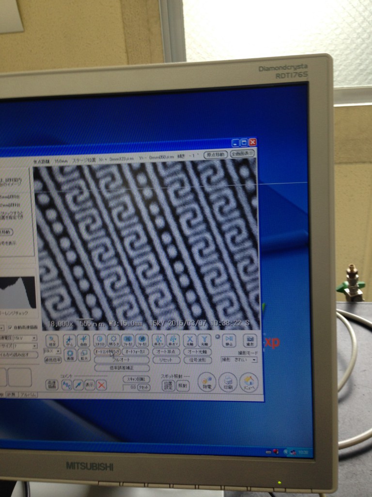
Next it was onto the really interesting stuff, one of our group had extracted and mechanically decaped a GPU.

This was if I remember correctly part of what we think is the OTP ROM:

photo 1

At 9000x:

RAM:

photo 1(1)


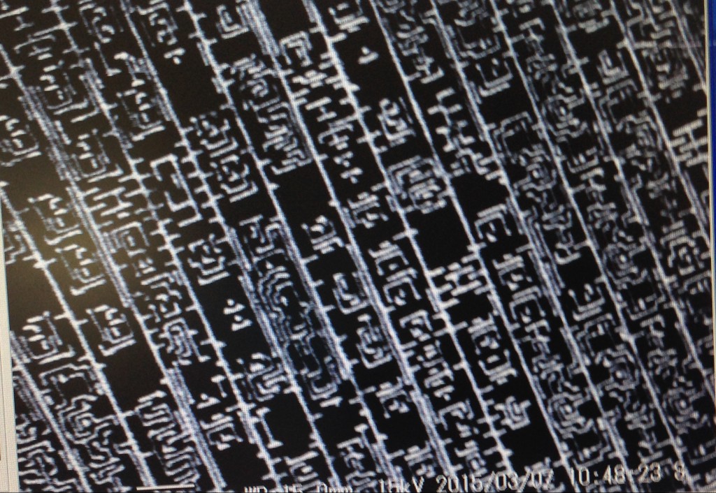
And some random logic:

photo 1(3)

Here we are at 100000x, the features here are ~50nm:

photo 3(3)

 
You can take a look at the pictures Marcan took here, much better than mine.

Elmo CCD Security camera

This is the second of the two security camera I picked up today, the first surprisingly contained a vidicon tube. However I was after a CCD to stick in a SEM and image tomorrow. Lucky the other camera I picked up had a CCD in it!

This was an Elmo security camera. Like almost all the cameras I’ve found in Japan it uses a Sony CCD and analog frontend. It’s pretty old and I’m guessing the features on the CCD should be clearly visible under a SEM.

photo 1

photo 1(1)

photo 2

photo 2(1)

photo 3

photo 3(1)

photo 4

photo 4(1)

photo 5

photo 5(1)