DDC112 Board Design/Bring Up
The DDC112 is a integrating current input ADC. You can use it for acquiring small currents (of the range of femto to picoamps (or larger if you want). Often a trans-impedance amplifier (current to voltage converter) would be used for this purpose. However the DDC112 doesn’t work like this…
The DDC112 collects current on a capacitor. It then periodically switches the capacitor over to a ADC, and starts collecting charge on a second capacitor while acquisition takes place. So, rather than having “gain” the switched current integrator has two parameters you can vary. The size of the capacitor and the time you integrate over.
The DDC112 has a number of build in capacitors, and you can also add your own externally. The DDC112 is really designed for photodiode applications. The series contains parts with 100s of channels, and built in ADCs. You’d use these for photodiode array systems, things like X-ray machines, CT Scanners etc.
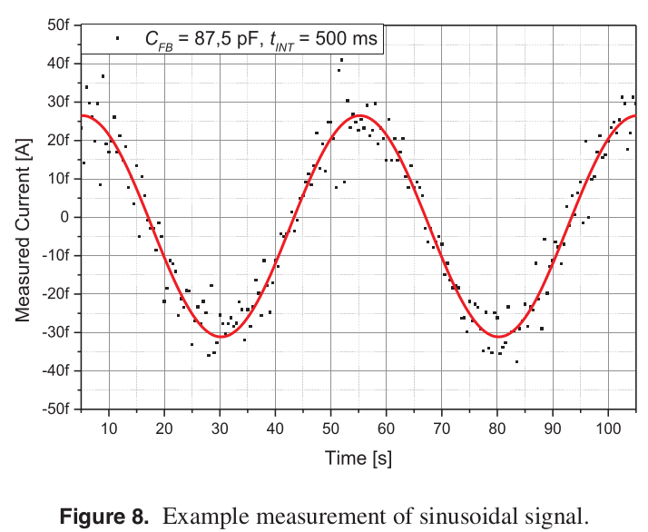
However, I’m more interested in alternative applications. Things like scanning tunneling microscopes, or nanopore systems. Both these applications require the acquisition of picoamp current traces at a few kilohertz. Googling around, I found an interesting paper where they evaluated the DDC112 for use in an STM. They show a 50 femtoamp sine wave (sampled at 2Hz) which I thought was pretty cool:
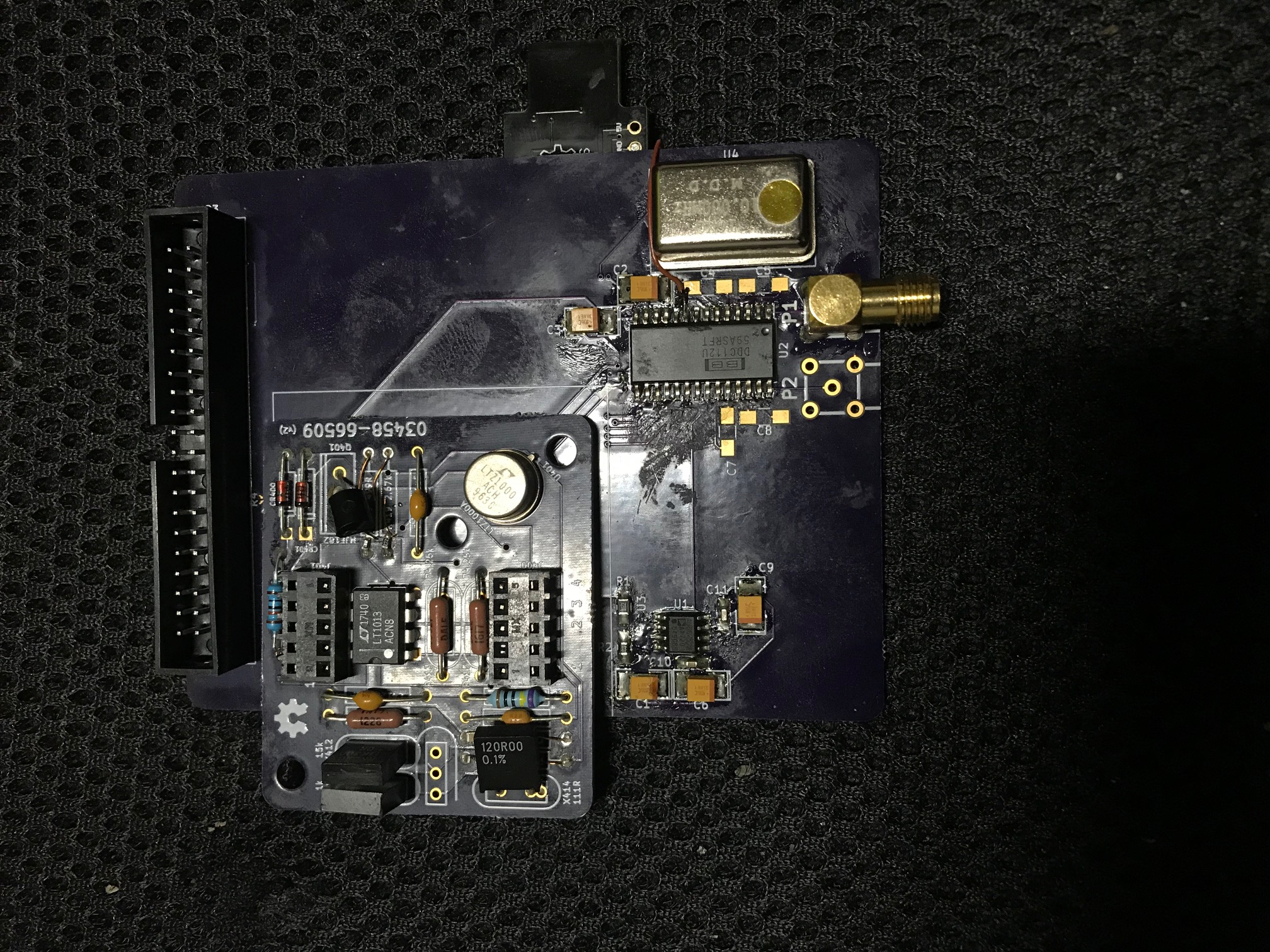
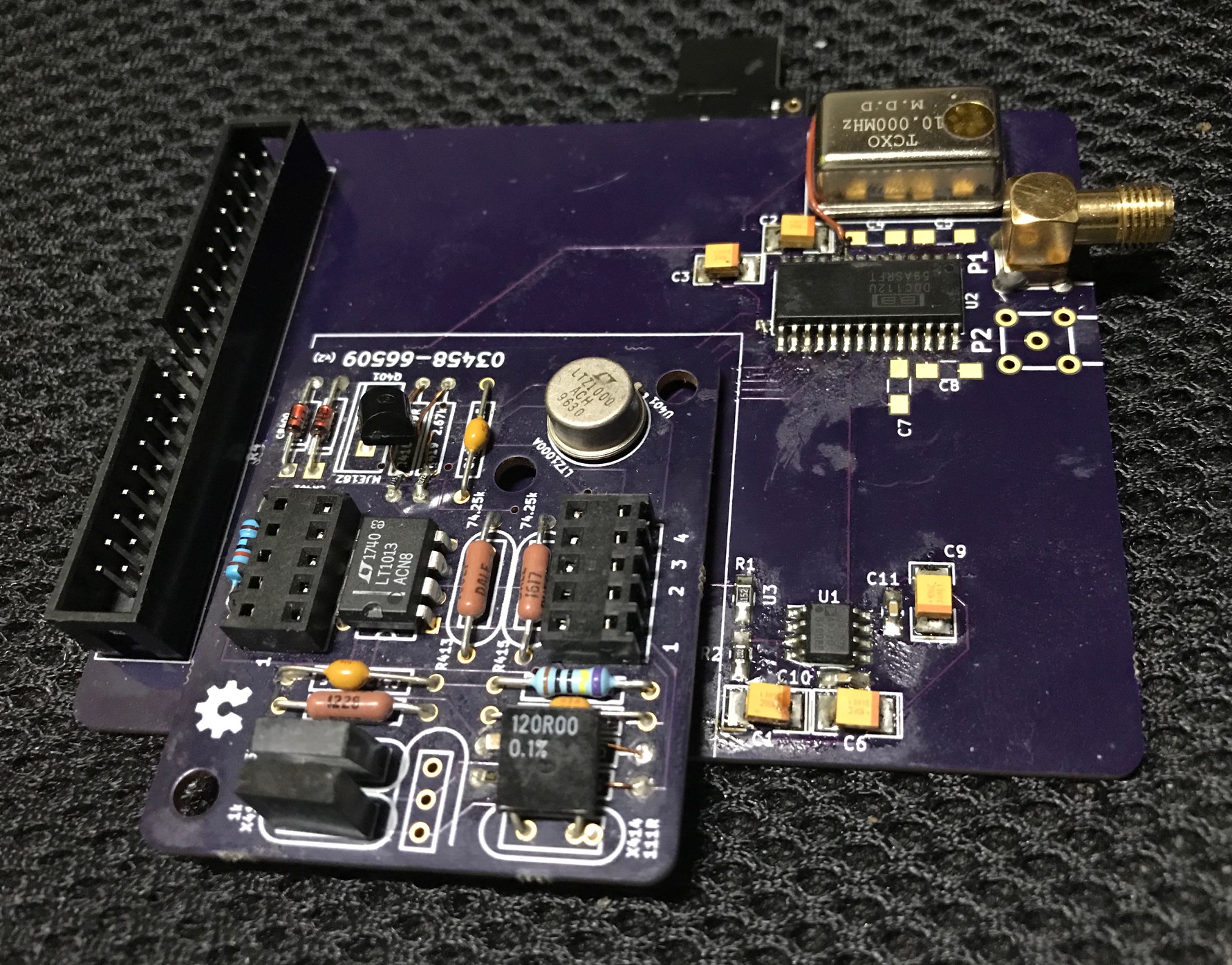
Various other sources indicated that you should be able to get about 2 picoamps of noise at 1KSPS. Unfortunately I’ve not seen any board designs or code generally available. So I’ve started putting my own design together and doing some basic testing. Here’s the completed board:
Everything is probably overkill here… The DDC112 requires a 10MHz clock, so I used a 10MHz TXCO… totally unnecessary. But I was curious to play with a TXCO. I may well end up swapping it out later.
The DDC112 has continuous and non-continuous modes of operation. I wanted to run in continuous mode, constantly taking samples. To do this, you need to toggle the CONV pin, at a fixed frequency. This controls the switching (switching between collecting charge on one capacitor or another).
This frequency should be somewhat synchronized with the main clock. If I was using a fast (>100MHz) processor, I could probably just synthesize the 10MHz clock and the CONV trace. But i wanted to retain flexibility (and have currently been driving the board with an Arduino Mega). For this reason I decided to add a clock divider/generator.
For this I used an ATTINY85. I modified a digispark to use the same oscillator as the DDC112 as documented here. Currently I’m using it to generate a 1Khz CONV signal.
With these two signals in place, the DDC12 will acquire data, and pull DVALID low when an acquisition is ready. You can use DVALID to trigger and interrupt, and transfer the data to a microprocessor over SPI.
I’ve included board designs, and a dump of the code I used for testing in the notes below. A number of hacks were required on the board (re-routing DVALID to an interrupt capable pin, adding the digipark frequency generator). But they’re here for reference.
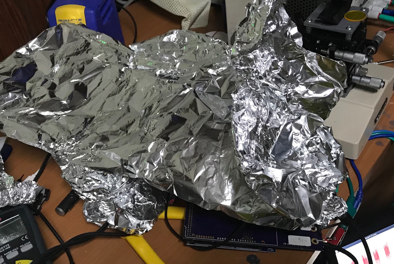
I’ve completed some very basic tests. The board seem capable of acquiring picoamp level signals. My shielding isn’t great:
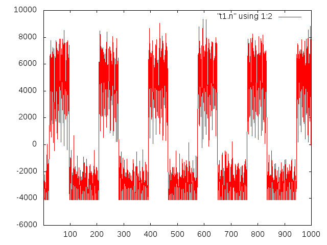
But the first traces don’t look too bad, here’s a 5Hz 1nA square wave, sampled at ~1.2KSPS:
And here’s a 200pA square wave at the same:
The 200pA trace isn’t as clean as I’d like it to be, but I think if I clean up my test setup I should be able to improve things. In particular, I’m using a 100MOhm resistor to generate in input current. Likely using a larger resistor (and larger/cleaner voltage over it) would help a little. Obviously the shielding and board layout also needs work.
If you have a potential application for this board, please contact me. It would be interesting to collaborate.
Notes
Board designs (unchecked): DDC112_boards.tar
Arduino Mega code:
#include#include void setup() { // put your setup code here, to run once: Serial.begin(115200); SPI.begin(); SPI.beginTransaction(SPISettings(10000000, MSBFIRST, SPI_MODE0)); // range pins pinMode(A7,OUTPUT); pinMode(A6,OUTPUT); pinMode(A5,OUTPUT); // range setting digitalWrite(A7,HIGH); digitalWrite(A6,LOW); digitalWrite(A5,LOW); pinMode(2,OUTPUT); //TEST pinMode(13,INPUT);//CLK pinMode(4,OUTPUT); //DXMIT digitalWrite(4,HIGH); pinMode(5,INPUT); //DVALID, old routing digitalWrite(2,LOW); //TEST PIN LOW=off attachInterrupt(1, read_data, FALLING); //DVALID (re-routed) } long int a=99; long int b=99; long int c=99; long int d=99; long int e=99; bool read_ok=false; long int in1 = 0; long int in2 = 0; void read_data() { // READ DATA digitalWrite(4,LOW); //DXMIT a=0; b=0; c=0; d=0; e=0; a = SPI.transfer(0); b = SPI.transfer(0); c = SPI.transfer(0); d = SPI.transfer(0); e = SPI.transfer(0); digitalWrite(4,HIGH); in2 = (a << 12) | (b << 4) | (c >> 4); in1 = ((c & 0x0F) << 16) | (d << 8) | e; in1 -= (1 << 12); in2 -= (1 << 12); read_ok=true; } void loop() { //1 DCLK_INF SCLK //2 DVALID_INF 3 (patch) //3 SDIN SDIN //4 DXMIT_INF 4 //5 DOUT_INF SDO //6 CONV_INF 3 //7 NC //8 TEST_INF 2 //9 NC //10 RANGE0_INF AD7 //11 NC //12 RANGE1_INF AD6 //13 NC //14 RANGE2_INF AD5 if(read_ok) { Serial.print(in2); Serial.print(" "); Serial.println(in1); read_ok=false; } }
ATTINY85 code:
void setup() {
  // put your setup code here, to run once:
  pinMode(PB0,OUTPUT);
}

void loop() {
  // put your main code here, to run repeatedly:
  for(;;) {
    digitalWrite(PB0,1);
    delayMicroseconds(500);
    digitalWrite(PB0,0);
    delayMicroseconds(500);
  }
}
