The esp32 wroom32 design
Espressif kindly provide the schematics and layout files for the esp32 based WROOM32. In preparation for my own design (based on my espusb) I’ve been looking over these files.
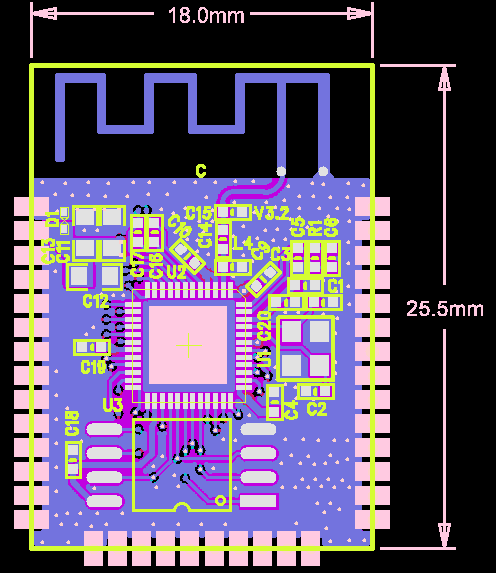
The zip file they provide (local copy) contains 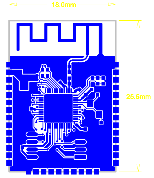 design files in a variety of formats. The source .PCB and .SCH files appear to be included, but there are no notes and I couldn’t determine which tool they are for (if you know please comment – my best guess is OrCAD). They also include pdf printouts of the schematic and and layout. The Layout pdf is reproduced to the right. However, it doesn’t show any of the silk and only appears to be the top copper layer. I therefore generated the image above from the gerbers that are also included.
The gerbers also don’t use a naming convention I’m familiar with, but from what I can tell the WROOM32 is a 4 layer board. I’m kind of surprised that they didn’t try and squeeze everything onto 2 layers, like they do with the esp1. Will be interesting to see if the esp32 also forces me to start doing 4 layer designs.
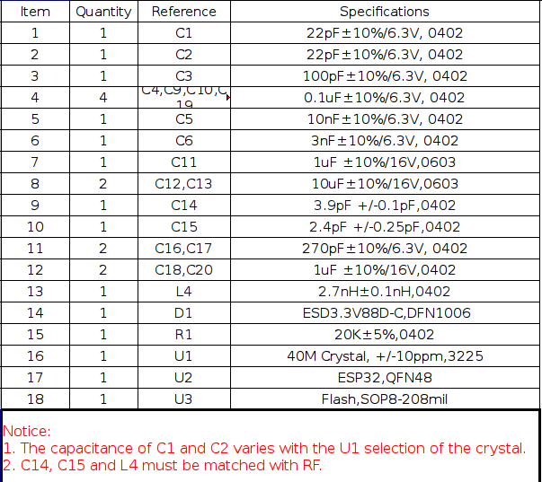
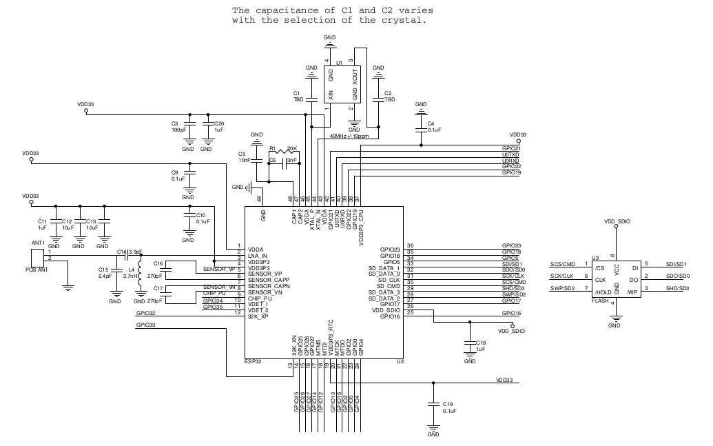
For reference, the BOM and schematic are below:
Last time I checked, we use OrCad and PADS, so the files probably are in these formats. We chose a 4-layer board so we can have a good ground plane, which helps with signal integrity, EMI etc. Fyi the ESP01 is not our design; it’s a board designed by AI-Thinker. If memory serves, for the later boards they produced (eg the later ESP12 boards) they also switched to 4-layer PCBs.
Thanks, I’ll see if I can try PADS. Also thanks for the other info. btw, I tried to contact you a while back about your TSOP48 NAND flash reader (I’ve laid it out on a PCB). Be great to chat further: [email protected]