ESP8266 – esp1 PCB scans
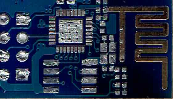
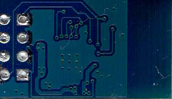
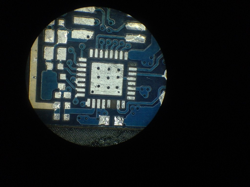
There are some partial layout images for the esp1 but they seem incomplete. I wanted to make sure I knew exactly what was going on with this layout and as they’re so cheap decided to pull the components off a board and scan it. Actually a little pointless, as I was wondering if there was a trace snaking under the chip, but nope! Anyway, for reference, here are the scan images:


Nice.. thanks for sharing
Thank to your photos i can add three more pins to an esp01, gpio12, gpio13 and gpio14. Insane soldering job!