TDS2024 Images
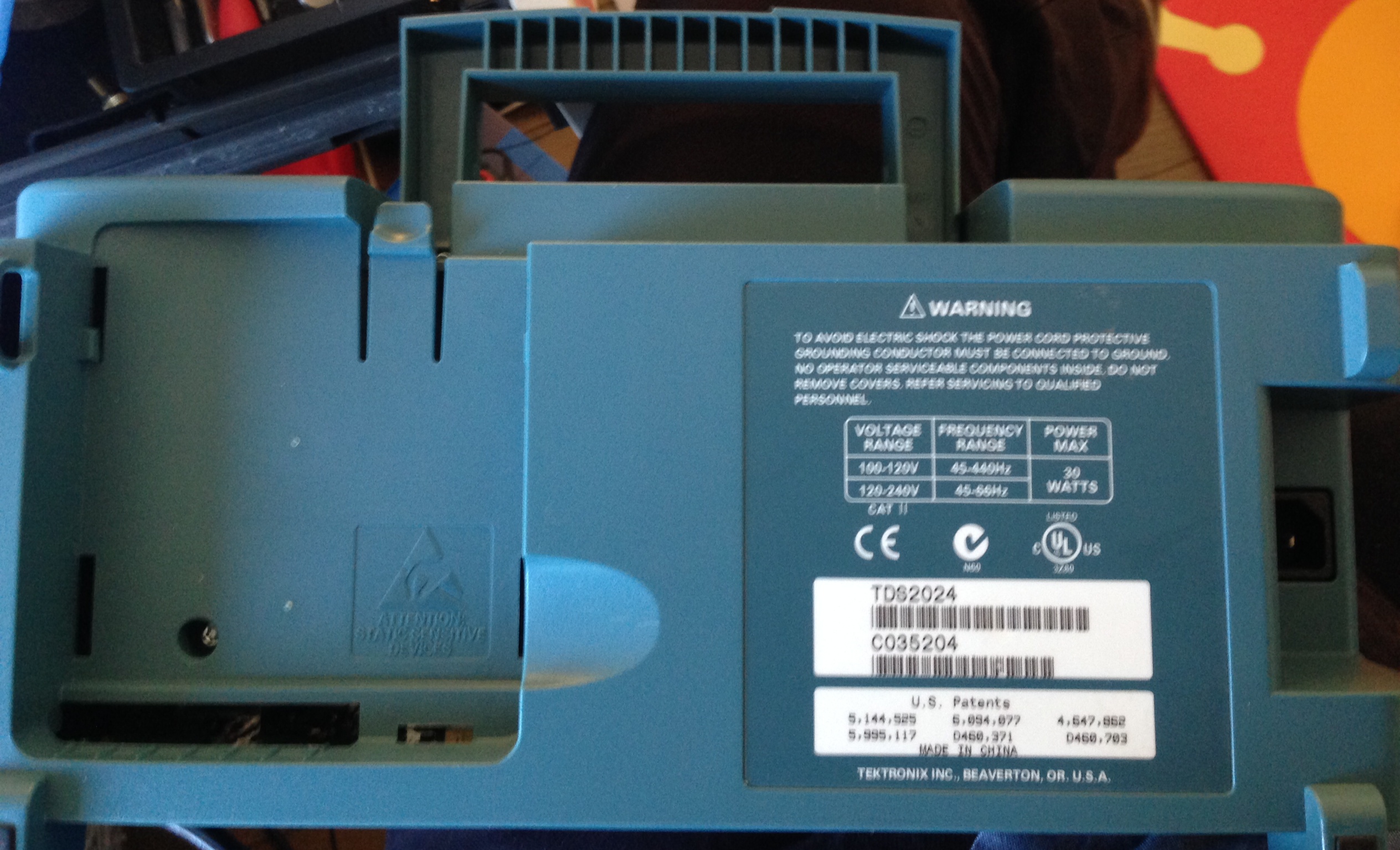
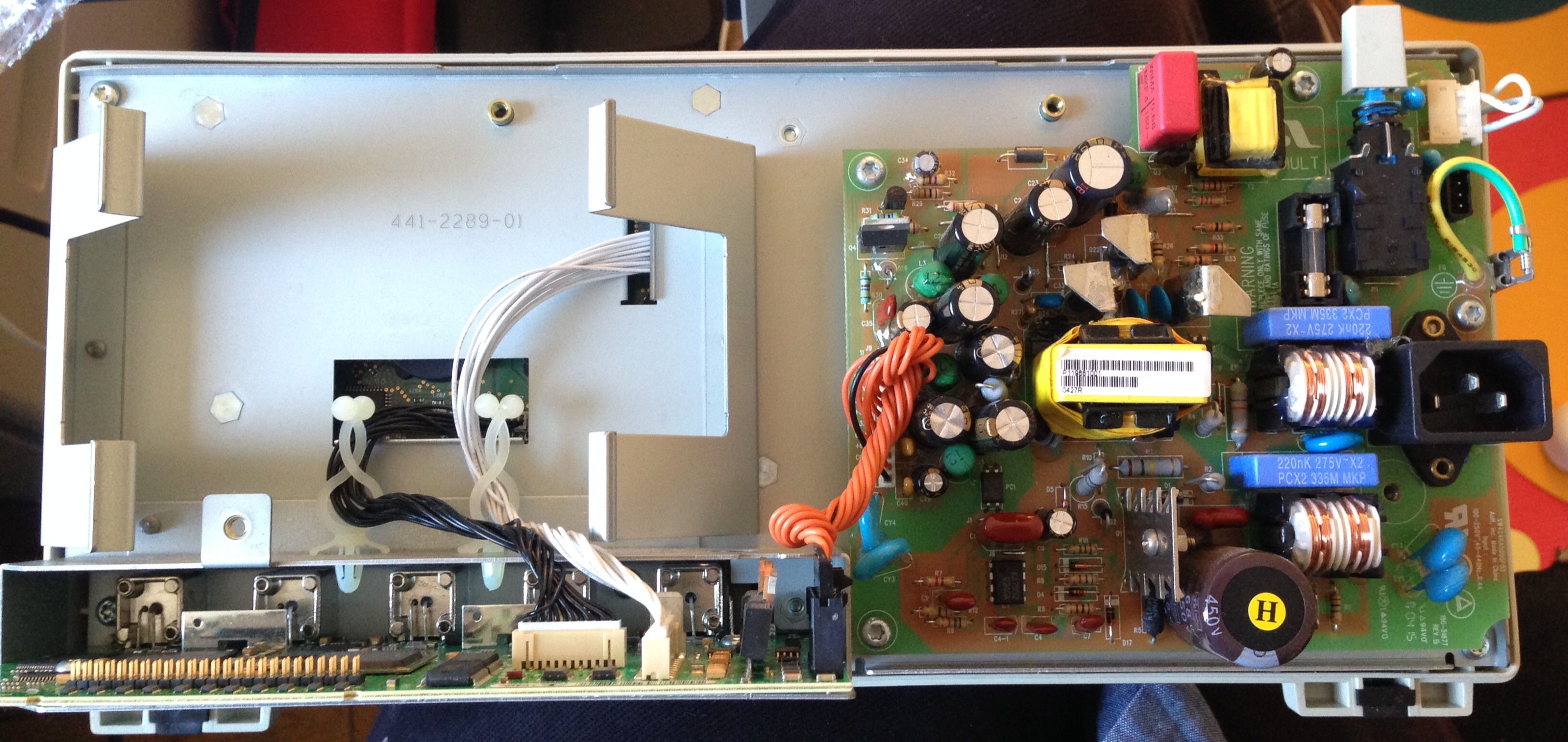
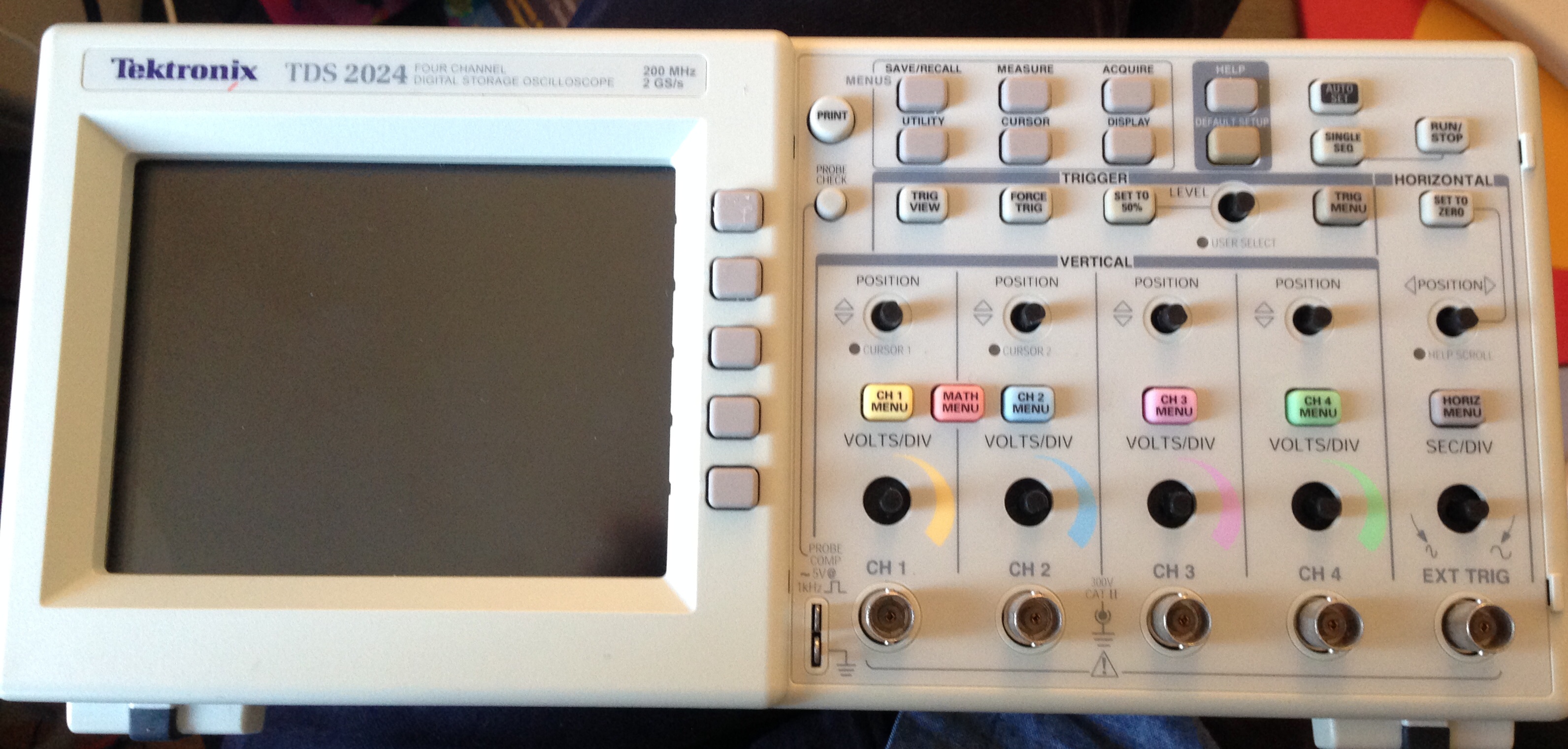
In preparation for a basic repair (screen replacement). I’ve taken some internal and external pics of the TDS2024 I picked up on an auction. Here they are!


My contribution to the increasing entropy, and eventual heat death of the universe
In preparation for a basic repair (screen replacement). I’ve taken some internal and external pics of the TDS2024 I picked up on an auction. Here they are!
UPDATE: I’d recommend checking out Gorilla Websockets for golang, the standard library doesn’t support things like KeepAlive packets making it pretty difficult to use in practice.
This is a simple example of websocket communication in golang. Two files are required the golang go and a index.html file which it will server. Here’s the golang:
package main

import (
	"code.google.com/p/go.net/websocket"
	"io"
	"net/http"
	"fmt"
)

func echoHandler(ws *websocket.Conn) {

  receivedtext := make([]byte, 100)

   n,err := ws.Read(receivedtext)

  if err != nil {
    fmt.Printf("Received: %d bytes\n",n)
  }

  s := string(receivedtext[:n])
  fmt.Printf("Received: %d bytes: %s\n",n,s)
  io.Copy(ws, ws)
  fmt.Printf("Sent: %s\n",s)
}

func main() {
  http.Handle("/echo", websocket.Handler(echoHandler))
  http.Handle("/", http.FileServer(http.Dir(".")))
  err := http.ListenAndServe(":8080", nil)
  if err != nil {
    panic("Error: " + err.Error())
  }
}
And here’s the html, the html file needs to be saved in a file called index.html:
<html>
<head>
<meta charset="UTF-8" />
<script>

  var serversocket = new WebSocket("ws://localhost:8080/echo");

  serversocket.onopen = function() {
    serversocket.send("Connection init");
  }

  // Write message on receive
  serversocket.onmessage = function(e) {
    document.getElementById('comms').innerHTML += "Received: " + e.data + "<br>";
  };

  function senddata() {
     var data = document.getElementById('sendtext').value;
     serversocket.send(data);
     document.getElementById('comms').innerHTML += "Sent: " + data + "<br>";
  }

</script>

</head>
<body>
  <input id="sendtext" type="text" />
  <input type="button" id="sendBtn" value="send" onclick="senddata()"></input>

  <div id='comms'></div>

</body>
</html>
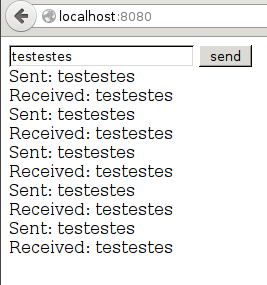
Once created you can run the golang with “go run main.go”. And goto localhost:8080 in your web browser to access the test site. If you don’t already have the library you may also need to download it with “go get code.google.com/p/go.net/websocket”.
While the above example works, it’s probably better to keep the socket alive. In the above example the Golang server will keep the socket alive for one read and one write, and then exit. The following example keeps the handler alive in a loop:
package main

import (
    "golang.org/x/net/websocket"
//    "code.google.com/p/go.net/websocket"
//    "io"
    "net/http"
    "fmt"
)

func echoHandler(ws *websocket.Conn) {

  for {
    receivedtext := make([]byte, 100)

    n,err := ws.Read(receivedtext)

    if err != nil {
      fmt.Printf("Received: %d bytes\n",n)
    }

    s := string(receivedtext[:n])
    fmt.Printf("Received: %d bytes: %s\n",n,s)
    //io.Copy(ws, ws)
    //fmt.Printf("Sent: %s\n",s)
  }
}

func main() {
  http.Handle("/echo", websocket.Handler(echoHandler))
  http.Handle("/", http.FileServer(http.Dir(".")))
  err := http.ListenAndServe(":8080", nil)
  if err != nil {
    panic("Error: " + err.Error())
  }
}
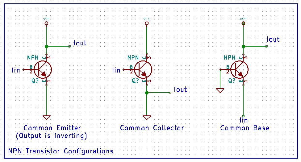
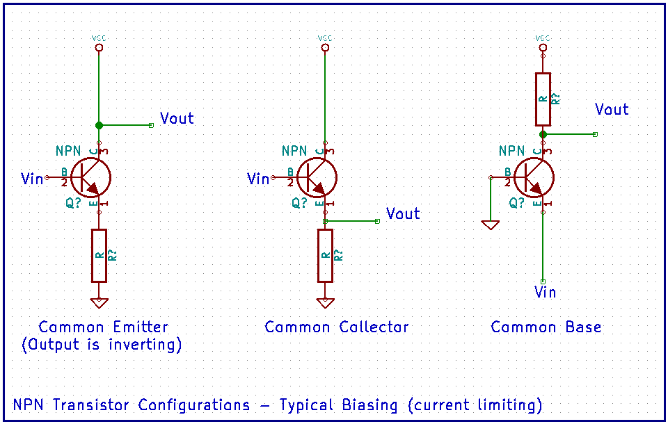
I’ve been learning more about different NPN transistor configurations and created the following diagrams for my own reference. The first shows where signal enter and exit the different configurations, but includes no current limiting. As such I’ve labeled the input and output signals I, for current. The second shows how current limiting might typically be introduced.
I’ve a long standing interest in STM projects since seeing the various low cost and amateur project attempts many years ago. I recently came across this paper describing a method for compensating for the probe vibration. The results (shown on HOGP below) see quite impressive. And allow for a scan rate of a few hundred Hertz.
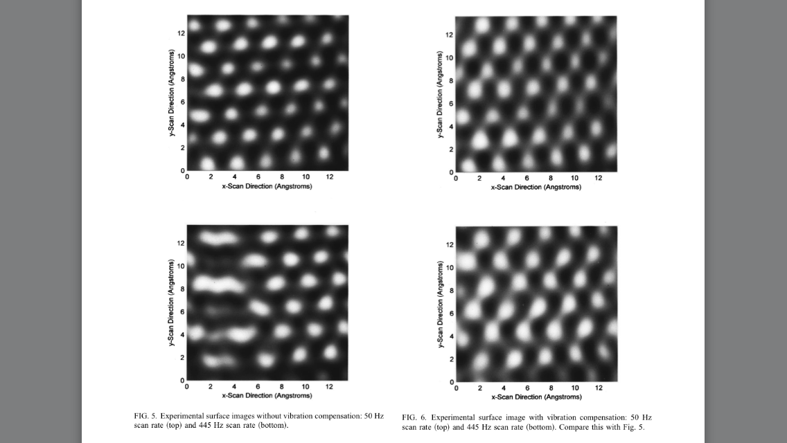
Vibration compensation for high speed scanning tunneling microscopy
D. Croft and S. Devasia,
Rev. Sci. Instrum. 70, 4600 (1999)
 RSS
RSS