Early promo shot from the old Solexa site. The 90s rocked!
In this post I describe non-technical aspects of the development of the Solexa sequencing platform. For those who don’t know, Solexa is the company that was acquired by Illumina. They developed (acquiring the necessary IP as required) a DNA sequencing platform several orders of magnitude faster and cheaper than what was previously available. The core chemistry developed at Solexa returns broadly similar to that currently used by Illumina, and which dominates the DNA sequencing market. If we decided to implement GATTACA today, you’d probably use Illumina machines.
Solexa are now long gone of course, the solexa.com now proudly boasts an exciting deep clean make up remover. Old versions are available via the waybackmachine.

Kind of a shame Illumina didn’t keep the domain…
It’s interesting to look at how things played out financially. And what it cost to get to each milestone. In this post I’ve pulled some data out of their filings with companies house, and a SEC filing which describes their technological progress.
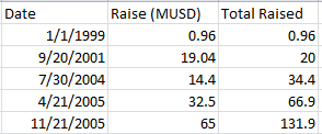
Briefly the following table describes the funding I’ve seen noted in the accounts and press releases (this maybe wrong and I’d welcome corrections):
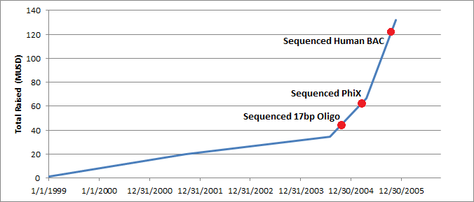
It’s instructive to plot this against certain milestones. These are available in a Solexa SEC filing. You can see that they’d raised 34.4MUSD in total prior to sequencing anything at all. Getting the platform up and running, took time. The sequencing milestone is 9 months after they acquired the Manteia cluster amplification IP which proved critical. Things moved rapidly after this point.
The total amount raised tells us something about how much it cost to develop the technology. It doesn’t however tell us about the valuation of the platform at each round. If you just plot the amount raised (rather than the total) you get the following:
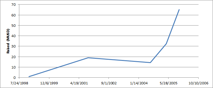
The fact that the raise in 2004 was lower than the previous value makes me suspect that it could have been a down round? Based on the numbers calculated in the section below I don’t think so. The valuation possibly looked like this:
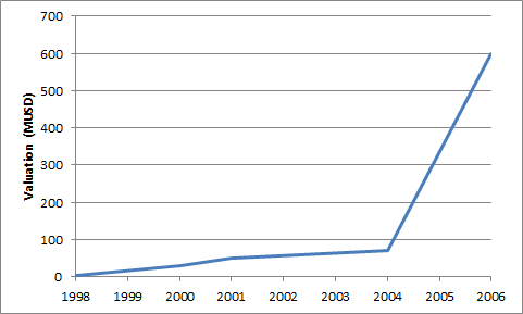
The interesting thing about this is that the valuation prior to a proof of concept looks like it was in the ~30->60MUSD range. After getting sequence data the valuation must have increased rapidly. It feels like the acquisition price was quite low, and that it could have been single digit multiples of the last round valuation. So, those are my thoughts on Solexa’s valuation and fund raising, I will try and rework this and check/fix the calculations when I can. Below I detail some the background/sources and how I arrived at some of the numbers above.
Business Development Background and Sources
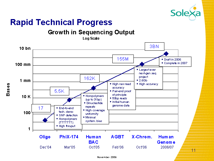
Progress in data generation at Solexa from 1.
The company was incorporated in 1998 as “Intercede 1356 Limited”. As a UK based company all its prior accounts are a matter of public record. However you’ll now have to search under “Illumina Cambridge Limited” (the business unit Solexa became after acquisition).
Their initial funding came from Abingworth Bioventures II. The first set of accounts filed shows 300KGBP in cash and records a 300KGBP loss (it records transactions to the end of 1999). The company commenced activities on the 12 of October 1998. And I would expect this raise to have been around that point.
The year 2000 accounts are a little more explicit, and contain the following statement:
REVIEW OF THE BUSINESS AND FUTURE DEVELOPMENTS
The Company has been established to undertake research and put the results of such research to commercial use.
The Company raised a further £1.5 million during the year by way of a convertible loan from Abingworth Bioventures II SICAV (see note 8 to the accounts). This has been used to establish the Company in its own premises and to build the management and scientific teams. Good progress has been made in the development of the Company’s proprietary single molecule technology.
EVENTS SINCE THE BALANCE SHEET DATE
Subsequent to the year end the company raise £100,000 by way of a convertible loan from the University of Cambridge.
On 20 September 2001, the capital element of the above convertible loans of £1.6 million from Abingworth Bioventures II SICAV and University of Cambridge were converted into 800,000 ordinary shares of 0.25p each at £2 per share. In addition £4,104 of accrued interest on the University of Cambridge loan was converted into 2,052 shares at the same rate.
Also on 20 September 2001, the company raised £12,000,000 (before expenses) by the issue of 4,000,000 ‘A’ ordinary shares of 0.25p each at £3 per share.
So by my reading there was an initial investment of 600KGBP in 1999. Sometime in 2000 they got an additional 1.5MGBP from Abingworth. Then in 2001 an additional investment of 13.6MGBP. It’s also an interesting technical note that they describe themselves as a single-molecule sequencing company.
Going through the accounts the next interesting event is the acquisition of the Manteia IP:
On 25 March 2004, Solexa Ltd and Lynx Therapeutics Inc. jointly acquired from Manteia SA the rights to propriety technology assets for DNA colony generation. Solexa intends to use the Intellectual Property, in conjunction with its existing technology for the comprehensive and economical analysis of individual genomes.
This was the point that they transitioned from being a single molecule company to a cluster (or as they called it at the time colony) based sequencing platform. For those familiar with the technical aspects of the system this, is a significant change in direction for the company.
Prior to 2004 they were burning about 3 million a year it seems. In 2004 they were burning about 5 million (GBP). By my reading of the accounts they had about 5MGBP left in the bank, that’s after raising what looks like 8MGBP:
On 30 July 2004 the Company issued 4,166,666 ‘B’ preferred shares with an aggregate nominal value of £10,471 for gross proceeds of £7,500,00. On 18 October 2004 the Company issued a further 277,778 ‘B’ preferred shares with an aggregate nominal value of £694 for gross proceeds of £500,000.
That was probably raised from Amadeus (as noted in this press release), in fact the Amadeus press release notes 14.4MUSD which is almost exactly 8MGBP at that dates exchange rate. The press release also notes that in total Solexa had raised 40MUSD to date. The exchange rate in 2004 was almost 2 dollars to the pound, so this approximately matches the 22.2MGBP if you total up what I found in the accounts.
In March 2005 they were acquired by Lynx Therapeutics, Inc.. While structured as an acquisition, it was more like a merger (or Solexa acquiring Lynx) Lynx changed its name to Solexa, Inc continuing the Solexa brand. The deal was possibly largely done to give Solexa a US stock listing. I believe most of the tech development was still done by the Solexa guys in Cambridge.
Because of the merger, the UK accounts are less informative from this point on. But we can see that in 2005 they burnt 9MGBP. The accounts state they have 8MGBP left in the bank. And 2006 they appear to have burnt about 13.5MGBP. And in 2007 they were acquired by Illumina for what was widely reported as being 600MUSD.
Other sources of information help fill in the gaps. A press release from July 12 2005 contains the following:
Solexa Completes $24 Million Private Equity Financing
HAYWARD, Calif.–(BUSINESS WIRE)–July 12, 2005–Solexa, Inc. (NASDAQ:SLXA) today announced that it has completed a private equity placement for approximately $24 million following stockholder approval of the financing at the Annual Meeting of Stockholders held on July 7, 2005. The financing represented the second and final closing of the $32.5 million private equity placement that was announced on April 21, 2005. SG Cowen & Co., LLC served as the exclusive placement agent for the transaction.
“This financing demonstrates our investors’ confidence in our ability to execute on our business plan to develop and market our next-generation sequencing systems based on Sequencing-by-Synthesis (SBS) and Cluster molecular arrays,” said John West, Solexa’s chief executive officer. “In the coming months, as we move closer to product launch, we expect to be able to announce additional experimental results demonstrating the performance of our platform in high-end genetic applications.”
Under terms of the financing, the second closing included the sale of approximately 6.0 million shares of common stock at $4.00 per share and issuance of warrants to purchase up to approximately 3.0 million shares of common stock at an exercise price of $5.00 per share. The first closing of the private equity placement, completed April 25, 2005, generated proceeds of approximately $8.5 million from the sale of approximately 2.1 million shares of common stock and approximately 1.1 million warrants. As previously announced, Solexa’s prior venture capital investors Abingworth Management Limited, Amadeus Capital Partners Limited, Oxford Bioscience Partners and SV Life Sciences invested a total of approximately $10.8 million in the financing at the second closing.
Stockholders at the company’s annual meeting also approved all other items included in the company’s 2005 Proxy Statement. Among the measures were the election of seven nominees to serve on the Solexa board of directors for the ensuing year, including three affiliated with the company’s venture capital investors and one with ValueAct Capital, the lead investor in the private equity financing. Other approved proposals included adoption of the company’s 2005 Equity Incentive Plan.
Their early press release contains the same information:
HAYWARD, Calif.–(BUSINESS WIRE)–April 22, 2005–Solexa, Inc. (Nasdaq:SLXA) today announced that it has entered into a definitive agreement for a $32.5 million private sale of common stock and warrants for the purchase of common stock with a group of leading institutional investors in the health care sector. The transaction is led by ValueAct Capital. Solexa also announced that G. Mason Morfit, CFA, a partner of ValueAct Capital, has been appointed to its board of directors, bringing board membership to eight.
Under terms of the financing, Solexa will sell approximately 8.1 million shares of common stock at $4.00 per share and will issue warrants to purchase approximately 4.1 million shares of common stock at an exercise price of $5.00 per share. Approximately 2.1 million shares of common stock and approximately 1.1 million warrants will be issued in a closing expected on or about April 25, 2005, and the balance of approximately 6.0 million shares of common stock and warrants to purchase approximately 3.0 million shares of common stock will be issued on the same terms in a second closing subject to stockholder approval at the 2005 annual meeting. Solexa’s intended use of proceeds includes the development and launch of its first-generation Sequencing-by-Synthesis (SBS) molecular array platform for genetic analysis and repayment of its loan from Silicon Valley Bank. All of Solexa’s previous venture capital investors, including funds affiliated with Abingworth Management Limited, Amadeus Capital Partners Limited, Oxford Bioscience Partners and SV Life Sciences, will be investing a total of approximately $10.8 million in the financing at the second closing of the financing and have entered into agreements with Solexa to vote in favor of the financing at the 2005 annual meeting. SG Cowen & Co., LLC served as the exclusive placement agent for the transaction.
A press release from 11/21/05 contains the following statement:
Solexa Announces Agreement for $65 Million Private Placement
HAYWARD, Calif. and CAMBRIDGE, England–(BUSINESS WIRE)–Nov. 21, 2005–Solexa, Inc. (Nasdaq:SLXA) today announced that it has entered into a definitive agreement with a group of institutional investors to raise approximately $65 million from the private sale of common stock and warrants for the purchase of common stock. This financing will result in net proceeds to Solexa of approximately $61 million after deduction of offering expenses.
Under the terms of the financing, Solexa will sell 10.0 million shares of common stock at $6.50 per share and will issue warrants to purchase approximately 3.5 million shares of common stock at an exercise price of $7.50 per share. Approximately 3.9 million shares of common stock and approximately 1.3 million warrants will be issued in a closing expected on or about November 22, 2005, and the balance of approximately 6.1 million shares of common stock and warrants to purchase approximately 2.2 million shares of common stock will be issued on the same terms in a second closing subject to stockholder approval.
So that’s 97.5MUSD in 2005. I don’t see anything else prior to the acquisition. The final data (used for the table shown above is then):
1999 960,000USD (600,000GBP*1.6)
2001 19,040,000USD (13,600,000GBP*1.4)
2004 14,400,000MUSD (8,000,000GBP*1.8)
2005 97,000,000USD
2007 acquired for 600,000,000USD
It would be nice to get some idea of the valuation at various points. UK companies also publish share ownership. So we can roughly work this out. In the first filing in 1999 Abingworth owned exactly 50% of the company. For which they seem to have paid ~1MUSD. Valuing the company at 2MUSD. They received an additional 1.5MGBP from Abingworth sometime in 2000 increasing the stake to 60%. Valuing the company at up to 30MUSD (depending on how exactly these two investments were structured).
After this round a bunch of people jumped in. Amadeus, Oxford Bioscience, mRNA Fund II, Scroder Ventures, SITCO, and SV all invested in a 20.04MUSD round. The 2002 return shows that Abingworths stake dropped to 47%. I don’t think Abingworth put much in, so I’d guess the valuation here was around 50MUSD. After this round there was a round in 2004 which Amadeus led. If I’ve worked the numbers correctly then before/after that round ownership broke down as follows:
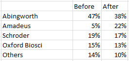
It looks to me like Amadeus put in basically all the cash. Other parties were largely diluted, though put in a small amount to help maintain stake. So of the 14.4MUSD I’m going to guess Amadeus put in 12MUSD. I should be able to work it more precisely but that ballpark, with a ballpark valuation for the company in the 30 to 60 million mark.
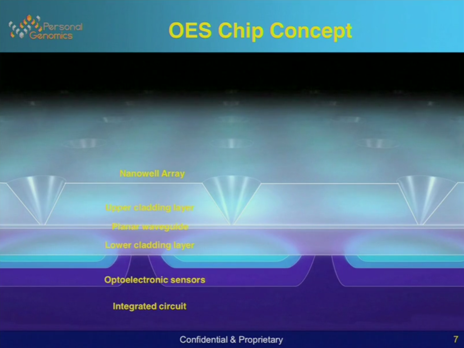
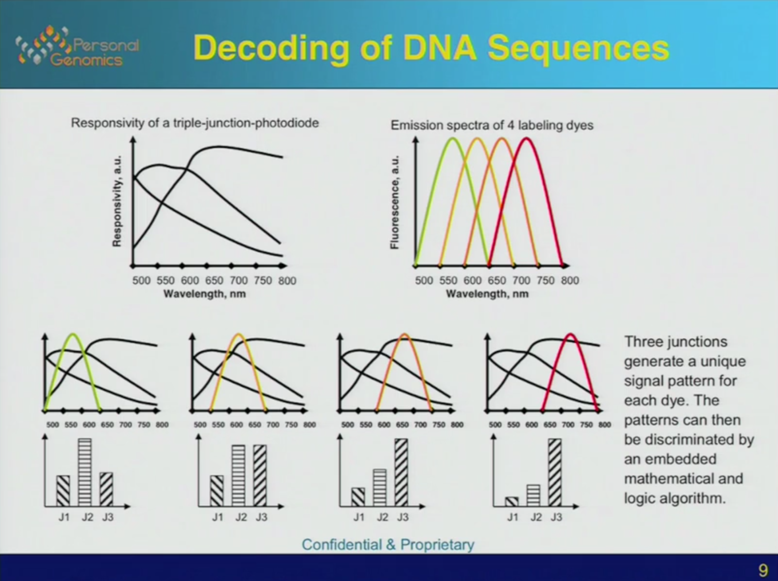
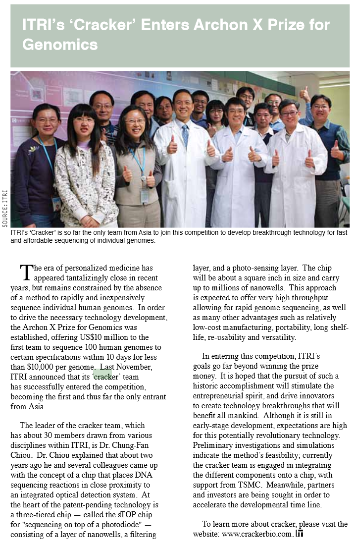 I recently came across a company called CrackerBio. They’d not come up on my radar before so I did some googling. As always, it’s worth noting that I have interests in this area and as such you should take my notes with a pinch of salt.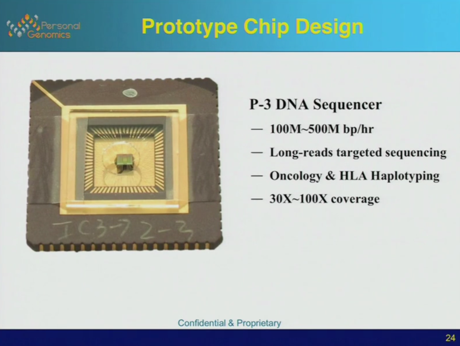

 RSS
RSS